- Three deposition technologies are available for depositing core layers of HJT structure – PECVD, CAT-CVD and PEALD
- PECVD is the most predominant technology of choice with several followers and suppliers
- CAT-CVD, employed during the early days of HJT development, but not so much during the current commercial phase, while innovative machine designs are in conceptual phase to overcome a few inherent limitations
- PEALD (Plasma Enhanced Atomic Layer Deposition), a new technology developed by Leadmicro is still under development.
Core layer depositions the heart of HJT processing. It involves multi-layer stacking of intrinsic-amorphous and doped-amorphous silicon layers of opposite polarities on each side of the wafer and controlling them at the nanometer scale. This is very important as the junction is created at the surface, and the deposited layers also dictate the effectiveness of passivation, which is key for the high performance of HJT. Not only in terms of performance, the core layer deposition tools also contribute as much as half of the CapEx required for the entire HJT cell processing line. PECVD and CAT-CVD, an abbreviation for catalytic chemical vapor deposition, have been the two main technologies of choice, while a new approach called plasma-enhanced atomic layer deposition (PEALD) has been introduced recently.
PECVD has been the predominant technology of choice here. However, the deposition technology has a vast field of applications, of which TFT display and very own amorphous silicon deposition tools from the past can also be tweaked for core layer deposition of HJT. Refurbished tools from both the streams have dominated the segment, especially during the initial development phase of HJT. It is the natural path followed by traditional thin-film PV companies that ventured into HJT, at least till the pilot phase. Companies like Hevel from Russia and Italy’s 3SUN, a subsidiary of Enel, belong to this category. Companies like Jinergy, CIC, Sunpreme also started their HJT projects with refurbished equipment originally developed for TFT. However, with HJT moving into the real commercial phase requiring high productivity systems, the companies are often relying on tool platforms developed specifically for PV. Today’s market offers a wide variety of PECVD tools that differ in RFs, plasma source technology, tool configurations such as cluster inline and intra-system transportation and number of vendors.
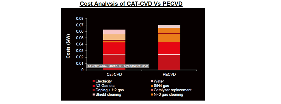
CAT-CVD, also known as hot-wire CVD, is also a widely used technology for core layer deposition. Since the processing environment is free from ion bombardment, the resultant film is believed to be of high quality. The technology also carries the legacy of being used by Panasonic. On the flip side, it is generally believed that increasing the throughput of the CAT-CVD tools is not easy and the tools themselves are known for not being handling-friendly, which means that automation costs are high. And due to the vertical processing design, breakages are also high. The hot wire “filament” requires special attention, involving higher maintenance costs. As of now, only Ulvac is offering a commercial scale production system based on CAT-CVD technology. However, according Hideki Matsumura from JAIST, who presented a detailed comparison of CAT-CVD with PECVD at the 3rd SHJ Workshop, CAT-CVD has lower manufacturing costs governed by the better utilization of precursor silane gas. Matsumura’s team has also been working on to overcome some of the limitations by adapting the technology on innovative machine design, but it’s still in the conceptual stage.
PEALD is a brand-new technology developed by China’s Leadmicro, which it presented at SNEC 2019 for the deposition of intrinsic and doped amorphous silicon layers for making heterojunction cells. According to the limited data available, plasma ignites hydrogen to strip the silane to deposit the amorphous silicon. The ability of the tool to accomplish in-situ doping that enables controlling the doping profile very precisely is the key competitive benefit of the tool, according to Leadmicro. While a system based on the same platform designed for depositing tunneling oxide and doped polysilicon for passivated contacts is already in production, the HJT solution is still under development.
For detailed analysis on core layer deposition technologies , please download and read TaiyangNews report on Heterojunction Solar Technology 2020, which can be downloaded for free here.

