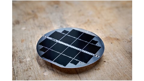

Germany's Fraunhofer Institute for Solar Energy Systems (ISE) has reported a new record efficiency of 25.9% for a III-V/Si tandem cell grown directly on silicon. It says the cell was produced on a low-cost silicon substrate for the first time which makes this an 'important milestone on the way to economical solutions for tandem photovoltaics'.
This is an improvement over a 24.3% efficiency level for III-V semiconductor layers of silicon solar cells the institute reported last year in August 2019 (see 34.1%: Monolithic Triple-Junction Solar Cell Efficiency).
Stating the reason behind this improvement in less than a year, Fraunhofer ISE Researcher Markus Feifel said, "This was achieved by replacing a single thin layer within the multi-junction cell. A careful analysis of our cells showed that this layer created a potential barrier for electrons moving through the crystal structure."
According to the institute, this improvement and this technology is ideally suited for electrolysis where solar power can be used to produce renewable hydrogen, touted as a building block for the energy transition.
"Not only are we working to make silicon solar cell production more sustainable and cost-effective, but we are also breaking new ground, added Prof. Dr. Stefan Glunz, Division Director of Photovoltaics Research at Fraunhofer ISE. "We are aiming to reach even higher efficiencies using tried and tested silicon in combination with other semiconductor materials and have achieved this in the field of tandem photovoltaics."
Researchers at the institute prefer a direct manufacturing process through which the III-V layers are deposited or grown directly onto a silicon solar cell, since the other process of transferring III-V semiconductor layers from a gallium arsenide to a silicon substrate then connected by wafer bonding is efficient, but an expensive way.