
- Markets
- Business
- People
- Opinion
- Technology
- Storage+
- Reports
- Our Events
- Tenders
- Price Index
- Top Modules
- ServicesServices
- AnalysisAnalysis

The study distinguishes between recombination and passivating pinholes at the SiOₓ interface
Pinholes are not uniformly detrimental; their impact depends on passivation quality
Process control of the SiOₓ/poly-Si interface remains critical for improving TOPCon performance
As TOPCon becomes the mainstream high-efficiency silicon solar cell architecture, attention is also turning to its underlying interface physics. At the core of this is the ultrathin silicon oxide (SiOₓ) layer and the doped polysilicon contact, which together govern carrier transport and recombination. During processing, microscopic pinholes form in the oxide layer and have traditionally been treated as defects that limit performance.
A joint research team from DAS Solar, Hebei University, and Forschungszentrum Jülich has examined this assumption. In a study published in Nature Communications, titled Passivating pinholes for large-area and high-efficiency silicon solar cells with tunnel oxide passivated contact, the researchers identify a class of interface features termed passivating pinholes. This research work provides additional insight into carrier transport and recombination behavior at the TOPCon interface.
Based on industrial TOPCon solar cells with a c-Si/SiOₓ/poly-Si structure, the work included an interface analysis carried out using Cs-corrected HAADF-STEM (High-Angle Annular Dark-Field Scanning Transmission Electron Microscopy), supported by EELS (Electron Energy Loss Spectroscopy) and electrical measurements to correlate nanoscale features with device performance.
Conventionally, pinholes in the SiOₓ layer have been treated as detrimental. They were associated with reduced passivation quality, increased recombination, and losses in open-circuit voltage (Voc). Since these pinholes were also considered unavoidable, they were seen as an intrinsic limitation to further performance improvements.
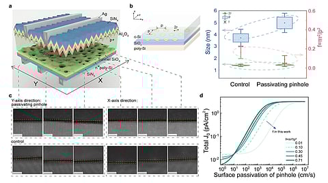
To better understand the role of pinholes at the interface, the researchers carried out atomic-scale characterization of the SiOₓ/Poly-Si structure. Using advanced electron microscopy and chemical analysis, the researchers examined the interface at the atomic scale and identified 2 types of pinholes.
The first type, referred to as recombination pinholes, shows oxygen depletion and direct silicon-polysilicon contact. These regions act as recombination centers, degrading device performance.
The second type is termed passivating pinholes. These regions retain sufficient oxygen despite local thinning of the oxide layer. This enables passivation of dangling bonds while allowing carriers to tunnel through. These features were observed at the nanoscale, with dimensions on the order of ~1-2 nm and high spatial density.
The findings indicate that not all pinholes behave the same. Their impact depends on their atomic configuration and chemical environment. Rather than being uniformly detrimental, their effect on device performance is linked to their passivation state.
Passivating pinholes combine 2 key functions: suppression of interface recombination and facilitation of carrier tunneling. This suggests that the presence of pinholes alone is not the defining factor. Instead of eliminating pinholes entirely, the results point toward controlling their properties.
This shifts attention toward interface engineering within the SiOₓ/Poly-Si stack. In particular, device performance appears to depend on balancing oxide thickness, oxygen content, and carrier tunneling.
From a manufacturing perspective, the study indicates that process conditions influence pinhole characteristics. This includes oxidation conditions and subsequent thermal steps. Parameters, such as oxidation temperature, duration, and ambient conditions, were shown to affect the formation and nature of pinholes.
Controlling interface conditions can support incremental improvements in open-circuit voltage and overall efficiency in large-area cells. The study reports 333.3 cm² TOPCon cells achieving 25.4% efficiency and open-circuit voltages approaching 739 mV under optimized conditions.
The work was supported by a provincial R&D program focused on linking fundamental research with industrial processes. DAS Solar and Hebei University have also established a joint research center to address device physics and manufacturing topics.
According to DAS Solar, its TOPCon production has exceeded 27% cell efficiency. The company is also developing back-contact technologies, with reported efficiencies above 27.7% at the cell level and over 24.8% at the module level.
