

Passivated contacts is a hot topic when it comes to advanced solar cell architectures. The basic principle of this cell structure is to apply metal contacts without patterning. In order to realize this in the real world, 2 steps are necessary – growth of interfacial oxide and deposition of intrinsic polycrystalline silicon layers, which is subsequently doped.
However, while each of these steps can be accomplished in a separate tool, there are also machine platforms that can accomplish all the steps in one machine. Thus, the count for the number of additional process steps varies according to the opted method and machines. Then, the number also changes according to the base process.
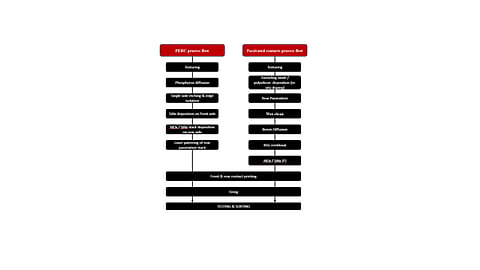
The additional steps described above are referring to a case when upgrading from n-PERT to passivated contacts, which every n-PERT maker will have to do eventually as the efficiency development with this technology is not competitive against today's new standard cell technology, PERC. When compared to PERC, boron diffusion and subsequent cleaning steps are added to the list. Even followed of traditional BSF cells can directly upgrade to passivated contacts, bypassing PERC.
There are several variants of the passivated contacts process flow. One way is to start with formation of the boron emitter, that's what the majority of the Chinese companies are doing. It is also possible to start the flow by accomplishing rear surface engineering first, followed by front side processing, which is promoted by French company SEMCO Smartech (see flowchart for details).
There is also a wide range of tunneling oxides to choose from. Fraunhofer ISE uses a wet-chemical method to generate an ultra-thin oxide. Subsequently, researchers have developed other methods – plasma-assisted oxidation, wet-chemical hydrochloric acid oxidation, wet-chemical nitric acid oxidation, thermal oxidation, and UV/O3 anodization.
Nonetheless, the thickness of the tunneling oxide is an important attribute. While there is no standard as of now, according to literature, tunneling becomes less likely in the case of thicker oxides, since tunneling is assumed to take place when the oxide is thin, say less than 2 nm. Having said that, it's not easy to control the oxide layer thickness using the wet-chemistry method, due to the formation of native oxide that could increase the thickness to 5 nm before the wafer is subjected to polysilicon deposition. The growth of native oxide also depends on the time the wafers have to wait in the queue before they are sent to subsequent polysilicon deposition, which is difficult to control.
From a passivation point of view the best oxide is thermally grown, according to the CEO of Semco Smartech, Raymond de Munnik. "It's just physics," he said (TaiyangNews talked to de Munnik about TOPCon in an interview). As for execution in production, it is better when oxide and polysilicon are applied in one go, if the tool platform permits. There is also an ambiguity with respect to the thickness of the polysilicon layer – it varies from 100 to 300 nm –, while the thickness also depends on the application method.
As TopCon uses silver on both sides, German company RENA advertises a plating approach to replace traditional screen printing. RENA SVP Technology and Innovation, Holger Kühnlein in an interview with TaiyangNews, said "For TOPCon, plating is extremely interesting, because today silver paste is required on both sides. The same rule also applies to n-PERT and SHJ. Moreover, a polysilicon passivation layer for TOPCon has to be quite thick to enable a fire-through paste metallization. Due to this, current TOPCon structures still suffer from low bifaciality, expensive Poly-Si / Capping layer deposition. Here, we can bring a technology that can get rid of very high silver consumption, bring down costs and improve bifaciality."
For details on further important aspects of passivated contacts technology, see TaiyangNews Report on High Efficiency Cell Technologies 2019, which can be downloaded for free.
