

TaiyangNews recent market survey on cell production survey features tools from various equipment suppliers; in our previous article published on this topic we provided details for ALD Systems For Aluminum Oxide Deposition. Now we look into PECVD systems. Any aluminum oxide requires a capping layer, and this is very obvious in the case of ALD. It requires a silicon nitride capping that is typically applied with PECVD, and PECVD scores high on this account. One inherent advantage of a PECVD system over ALD is its ability to deposit the silicon nitride capping layer on top of aluminum oxide in one system without breaking the vacuum. That means the whole rear passivation process for PERC is executed in one pass, something that holds true for all the listed products in this section.
A total of 8 products are listed in this part of the survey for aluminum oxide deposition system based on PECVD, and all of them are direct plasma based and are typical parallel-plate tube reactors.
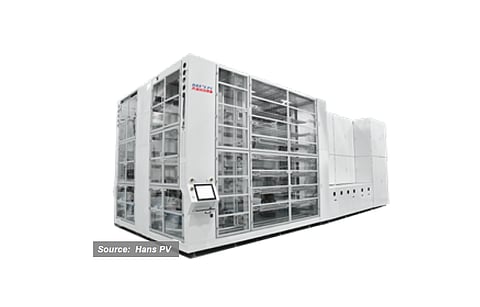
c.Plasma XL AlOx is the name of the latest PECVD tool from Centrotherm for this application. It is a 10-tube configuration with shared automation. This configuration offers redundant processing, as each of the tubes in the stack can be operated independently and each tube can be loaded with 416 M6, 350 M10 and 288 M12 wafers with about a 40-minute processing time. Following this sequence, the tool supports a net throughput of 6,500 wafers per hour.
Leadmicro is promoting a one of its kind PEALD / PECVD tool, which uses direct plasma energy for both ALD and CVD processes. Its ZR5000x2 utilizes PEALD for aluminum oxide deposition and PECVD for SiNx deposition. The system has 6 process chambers – 2 for aluminum oxide and 4 for silicon nitride deposition. The tool is compatible with M6 to G12 wafers, having a thickness of 140 to 170 μm. The cycle times for Alox and SiNx are 20 and 36 minutes, respectively. The system can process up to 5,670 wafers per hour (see Leadmicro Chief Scientist Baochen Liao Talked To TaiyangNews About The Key Enablers for TOPCon Cell Production).
S.C New Energy's direct plasma PECVD, based on parallel graphite plate technology, is offered in a 5-tube configuration. Each tube accommodates a boat with a capacity of either 558 pieces of M10 or 448 of G12 wafers, and processes them in a cycle time of about 40 minutes. The setup supports a throughput of 3,900 M10 and 3,200 G12 wafers per hour, respectively. At the end, the rear passivation stack deposited by its tools consists of 3 layers – aluminum oxide, silicon oxynitride and silicon nitride–, while the equipment is also capable of depositing the capping layer with a gradient refractive index, highlights the company.
Naura lists 5 products of its HORIS series with different suffixes. The latest among these are HORIS P12682 and HORIS P12642. These 2023 models are basically designed for larger wafer formats such as M10 and G12 and are also capable of handling thinner wafers of 125 μm with M10 size and 145 μm with G12. The major difference between these 2 similar looking systems is the number of wafers loaded per tube; 768 of M10 or 616 of G12 for HORIS P12682 and either 640 of M10 or 504 of G12 for HORIS P12642. Despite this difference, the tools strangely have the same throughput of 5,760 of M10 and 4,536 of G12 wafers per hour.
The remaining 3 – P12642M, P12622 and P12571M – respectively introduced in 2022, 2020 and 2019 are basically designed for all wafer sizes from M0 to G12 and thickness from 140 to 220 μm. They also differ in loading capacity – 640, 432 and 575 referring to M10 size – and support a throughput of 5,140, 3,394 and 3,687 wafers per hour, respectively. Note that the throughputs mentioned for all the tools discussed above are with reference to the deposition of aluminum oxide and the silicon nitride stack put together.
The article is an excerpt from the TaiyangNews Market Survey on Solar Cell Production Equipment 2023, which also includes detailed product specs and can be downloaded for free here.