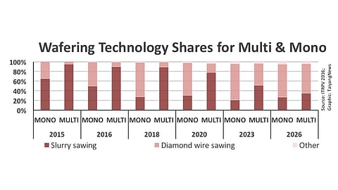

When taking a look in the newly released International Technology Roadmap for Photovoltaic (ITRPV) at all aspects related to producing wafers – such as employing diamond wire based sawing, potential to increase the throughput of sawing tools, reduction in kerf -, these have surpassed previous estimations or at least at the same levels. But progress related to the wafer as a product, such as thickness reduction, are delayed compared to the 2015 roadmap estimates.
Like last year, ITRPV's wafering section is showing several trends (see article Work in Progress in Wafering). On top, the current roadmap has provided more insight into recycling of silicon and diamond wire compared to the 2015 study, which skipped as many as 8 topics that were discussed in 2014's 5th edition. But one thing has not changed. Diamond wire based sawing remained at the center stage in the wafering section also in the current roadmap.
Diamond wire to dominate
Diamond wire based sawing is leading the technology development within the wafering segment. While slurry based sawing is still dominating, the acceptance of diamond wire based sawing is increasing due to its undeniable advantages. First and foremost is its high cutting speed, which is about twice that of the standard technology. The fixed abrasive principle makes the sawing free from usage of the grit and thus avoids the hassle of grit recycling as well as eradicates complex slurry management system at the factory level. This sawing method results in relatively lower kerf and also offers the possibility of using water as coolant that in turn eases the chances for recycling of silicon kerf. These advantages support diamond wire based sawing, which is quickly maturing in the monocrystalline wafering segment.
According to ITRPV's 7th edition, diamond wire based sawing for monocrystalline wafer slicing will dominate the market by doubling its share from 35% in 2015 to about 70% in 2018. Before that, fixed abrasive sawing is expected to attain equal presence as that of slurry technology already in 2016. This is an optimistic outlook about the technology over the past. While the 2015 roadmap has skipped the forecast for the monocrystalline wafering section, the 5th edition from 2014 expected it to be at about 30% in 2016. However, the 2015 roadmap has predicted diamond wire would replace slurry technology in 2024, whereas the current roadmap anticipates that standard technology would still be employed for producing about 30% mono wafers even after 10 years from now.
As for multicrystalline wafering, the application of diamond wire sawing is expected to gain acceptance despite the challenges, such as issues in texturing. ITRPV's view has not changed much about the subject. As already expected last year, it had a market share of about 5% in 2015 and would eventually dominate the slurry process by gaining 60% of the market in 2026, while the previous study allocated a slightly higher share of more than 50% by 2025.
Slurry fast in short term, but how?
The current roadmap is also upbeat about the potential for throughput enhancement for both sawing technologies – between 25% and 35% in the next 20 years -, while the 6th edition expected only a 20% to 25% improvement.
More interesting is that the slurry based process is considered to have slightly more upward potential to improve throughput in the short term compared to diamond wire technology. Taking the 2015 level as a reference, the throughput for both sawing technologies is expected to improve above 15% by 2020. However, slurry technology is anticipated to undergo a sharp rise in 2016, by 10%. From then no considerable improvement is expected until 2018, while the next improvement step would result in 115% in the next 2 years. On the other hand, the throughput of the fixed abrasive method is expected to raise progressively – 4% in 2016 and 9% in 2018. Then, both sawing processes are expected to gain 24% in throughput in the subsequent 3 years until 2023. By 2026, the diamond wire process would reach 135%, while the slurry-based method would only go slightly beyond 125%.
The roadmap, however, has not provided any details on methods or approaches on how to speed up slurry technology. Structured wire was considered to be a means of improving the throughput of the slurry technology, but the status of the technology is unclear after co-inventor and strong supporter of the technology, Applied Materials, announced to exit the solar wire sawing tools business last year.
High potential for kerf reduction
Increasing the thought is one way, while reducing the kerf loss also indirectly enhances the overall productivity of the sawing process. Kerf reduction increases the number of wafers produced per brick, which also reduces production costs. Kerf loss depends on the wire diameter and grit size of the slurry process; for diamond wire it is only about the effective wire (not just core wire) diameter. According to the 7th edition of ITRPV, as of today, kerf loss associated with slurry sawing is about 150 µm, whereas the diamond wire based process not only results in 25 µm lower kerf of 125 µm, but also has very high potential to go further down to 85 µm in the next 10 years. This actually indicates that developments in diamond wire sawing are exceeding expectations because the current roadmap estimates 40 µm reduction of kerf loss in 10 years, while the 6th edition estimated only 25 µm of kerf reduction.
Recycling of silicon gaining importance
Even when looking at small amounts – a loss is a loss, and kerf loss has a definite impact on costs. Diamond wire again comes for rescue. Not only does it waste less silicon, its fixed abrasive principle (not using silicon carbide grit) opens the possibilities for recycling silicon kerf. ITRPV has been emphasizing the importance of recycling of kerf silicon, but the 7th roadmap for the first time forecasted trends in silicon recycling. Kick started in 2015, silicon recycling is expected to attain a 15% share in 2018 and then become very prominent, surpassing 40% in the next 10 years. The diamond wire process offers another option of reducing consumables costs – recycling of the diamond wire itself. The current report expects diamond wire recycling to start in 2016, but stay low until 2020, when it is expected to attain close to 10%. In the subsequent 6 years, it would reach a significant level of 22% in 2026. Well established recycling of silicon carbide grit on the other hand has reached a threshold, though at a very high level, believes ITRPV – it already has attained a 80% share and is expected to stay at less than 90% over the coming 10 years.
Reducing kerf and even recycling kerf are still compromises in terms of silicon utilization, while advanced kerf-less wafering approaches eradicates kerf completely. Many startups, such as 1366 from the US or NexWafe from Germany are working in this direction. ITRPV has not changed its stance about the prospects of advanced wagering technologies. Like last year, the 2016 roadmap is not optimistic on alternative wafering approaches, which it expects to stay below 5% for the next 10 years. That's mainly because silicon is so cheap and the established sawing technologies are evolving so strong that they are creating a high level entry barrier for new technologies.
Wafer thickness reduction again on pause
While the above discussed aspects are about methods to produce a wafer, the silicon slice itself as a final product of this process has some important attributes. First, there is the wafer's contribution to the cell price, which has now reached a level of 61%, and thus a much higher share than the 51%, anticipated by last year's 6th edition. This is mainly due to a "supposed shortage of wafers, which" has lead to an increase in wafer prices.
This short impact aside, wafers still command a major chunk of the cell price – and reducing wafer thickness is considered to be an effective way to reduce cost. ITRPV has been a strong proponent of this approach in the past. However, all of its previous predictions about wafer thickness reduction, including the last one, have not come true. Falling polysilicon prices and the higher risk of breakage associated with thin wafers are hindering progression towards thinner slices. As a result, the preferred wafer thickness remained unchanged at around 180 µm since 2009.
In case of multicrystalline wafers, the expected wafer thickness in 2026 in the current roadmap is nearly the same as in the 2015 study – at about 150 µm; but the path is different. According to the present report, no considerable reduction in multi wafer thickness is expected until 2020 and a 10µm thinning is anticipated in 2020, 2023 and again in 2026, finally attaining 150 µm. The previous roadmap expected a consistent reduction from 170 µm in 2017 to 150 µm in 2022.
The 7th edition gives a rather conservative projection for monocrystalline wafer thickness reduction. It expect wafer thickness to drop to 160 µm by 2018, while the next 20 µm reduction would take about 8 years from then. The 6th edition expected this level to be reached in 2022 and 120 µm wafers to be common in 2025. Future module technologies, however, are expected to facilitate further reduction in wafer thickness, down to 100 µm in 2023, from 120 µm in 2020, 150 µm in 2018 and 160 µm tin 2016 – that's very close to predictions made a year ago.
No news on wafer shape
The shape of the wafer not only has an impact on material use but also on module efficiency – there's a reason why multi modules have similar efficiencies as mono modules despite lower cell efficiencies. Because multi slices are full square, mono wafers come with a pseudo square shape to avoid wafer damage during the special cutting process from monocrystalline ingots. As in the past, the ITRPV edition acknowledged the dominance of pseudo square mono wafers, at the same time being optimistic about the prospects for full square silicon slices in future. However, the 7th edition has not provided any forecast, while the 6th roadmap expected the share of full square wafers to increase 10 times in 10 years – from 2% in 2015 to 20% in 2025. Producing full square mono wafers would be much easier with advanced wafering techniques, such as kerf less approaches, but they are still in their infancy.
Apart from full square mono wafers and thickness reduction, the wafering segment – especially the topics associated with diamond wire based sawing – is advancing, in fact, more than expected in some instances. In diamond wire-based cutting, the potential for throughput enhancement and reduction in kerf are beyond ITRPV's earlier expectations. The possibility to recycle silicon kerf is a nice adder that comes with diamond wire based sawing.
