
Key takeaways:
DKEM presented low-etch pastes and multi-layer metallization approaches, including copper-based solutions
Cell makers are increasing emitter sheet resistance through shallow emitters and light doping, supported by weak-etch pastes
Fine-line and stencil printing are enabling narrower features, with ongoing experiments down to 4 μm openings
Fangqing Guo, New Technology Development Director at DKEM, presented the company’s latest metallization developments for TOPCon and back-contact (BC) cell architectures at the TaiyangNews Cell & Module Production Equipment & Processing Materials Virtual Conference.
He began by outlining DKEM’s product portfolio, which now covers pastes for PERC, TOPCon, BC, and heterojunction (HJT) cells, as well as materials for module interconnection and encapsulation. DKEM has recently introduced ‘silver-lean’ and ‘silver-free’ pastes to help reduce silver consumption. His presentation focused on metallization strategies for TOPCon and TOPCon-based architectures.
Guo stated that recent process developments have improved TOPCon cell efficiencies significantly. He elaborated on the methods of improvement for cell makers and on how DKEM supports these improvements.
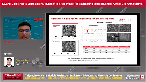
Cell manufacturers are optimizing the emitter layers to increase the sheet resistance (Rsheet) to 300-500 Ω per square. This is achieved by selecting a shallow emitter and light doping to increase the open circuit voltage (Voc). Guo highlighted that DKEM continues to support this increase in Voc by implementing and optimizing a weak etching system. This involves tuning the nature of the glass frit contained in the metallization paste. This weak- or low-etching, however, can create reliability issues due to the metal peeling off and yellowing.
Another development is ultra-fine line printing. Where screen openings were previously above 10 μm, many manufacturers now use openings narrower than 10 μm, and several have moved to <7 μm. Guo stated that DKEM and its customers are already experimenting with 4 μm openings, with the main challenge being maintaining sufficient paste deposition and long-term reliability due to the paste’s low laydown. Stencil printing was also presented as an option that can achieve narrower lines and improved morphology, but with cost and durability concerns. However, several companies have introduced stencil printing in mass production, and because of the advantages of this technique, there is scope for a 0.1% efficiency gain, according to Guo.
For the TOPCon rear side, with thinner polysilicon layers and selective rear-side structuring, pastes must maintain good contact formation while operating within low-etching regimes. Guo presented DKEM’s recent solutions designed to reduce etching depth, increase silver crystallite density, reduce the recombination current density at the metal contact (J0, m), and, most importantly, support stable printing performance. This is important because frequent screen changes in mass production lines can otherwise lead to efficiency losses if paste transfer and morphology are inconsistent.
For BC architectures, Guo noted that forming reliable contacts on the p-type polysilicon regions is a persistent challenge. As customers push toward thinner polysilicon layers, sometimes below 250 nm, the sensitivity to etching and contact formation increases. DKEM has worked to reduce crystallite size and increase packing density in the fired paste to maintain good contact and low resistance even at much lower polysilicon thicknesses. He reported that process and paste improvements now allow customers to reduce n-type polysilicon thickness to around 180 nm and p-type polysilicon to around 200 nm, with potential for further reductions.
He also discussed the potential shift toward copper as a replacement for silver, noting challenges such as oxidation, firing atmosphere sensitivity, and copper diffusion into silicon. DKEM is developing approaches using multi-layer metallization that combine a low-silver-content seed layer with a high-copper transport layer to reduce silver usage. Guo stated that this method is already in mass production for the rear side application in some TOPCon lines and has passed reliability testing. He concluded by saying that DKEM is working on new solutions for the TOPCon front as well.

