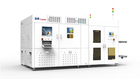


DR Laser presented laser-processing equipment for TOPCon poly-Si fingers and edge passivation
Both systems offer a throughput of up to 9,000 wafers/hour and support different wafer formats
The company also offers standalone and in-line laser patterning production equipment for BC cells
China-based laser equipment supplier DR Laser presented its latest laser-processing equipment for TOPCon and back-contact (BC) solar cell production.
DR Laser’s 4th-generation system uses laser processing to form selective poly-Si fingers on the rear of TOPCon cells. According to the company, the process provides an absolute gain in cell efficiency of 0.1-0.15% along with a 3-5% improvement in bifaciality. It adds that these gains have been demonstrated in mass production. The dual-lane system incorporates four laser sources that operate independently and offers a throughput of up to 9,000 wafers/hour. It supports different wafer formats, including rectangular and half-cut cells.
The company also presented edge passivation equipment for TOPCon cells. The laser process isolates the p-n junction from the cut edge, reducing recombination losses caused by cell cutting. The dual-lane system incorporates 2 independently operating laser sources and offers a throughput of up to 9,000 wafers/hour. It processes an edge width of 300-500 µm and supports rectangular wafers as well as half-cut and multi-cut cell designs. According to DR Laser, the process provides an absolute half-cell efficiency gain of 0.1-0.15% and increases the power output of a 2,382 × 1,134 mm module by 2 to 3 W.
For BC cell production, DR Laser presented laser-patterning equipment in standalone and in-line configurations. The platform integrates the laser process, optical design and patterning control, and is suitable for laboratory, pilot-line, and mass-production applications. According to the company, more than 1,000 of these units are operating in GW-scale BC cell production.
DR Laser also outlined its TOPCon technology roadmap. Its 5th-generation process combines laser-based local junction formation on the front, laser-induced firing, and selective tunneling contacts on the rear. The company is targeting cell efficiencies above 25.7% and expects the solution to become available within 2026.
