

HJT's unique structure, combining crystalline and thin-film silicon, has supported efficiency records
The move to double-sided microcrystalline silicon reduces parasitic absorption and resistance, improving fill factor and overall cell performance
High-mobility TCO materials developed by Risen enhance conductivity without sacrificing transparency
The most important attribute of HJT is that it is a fusion of wafer-based solar cell technology and thin-film PV, taking the best features from each. It has the excellent absorption properties of standard silicon wafer-based cells and superior passivation characteristics of thin-film amorphous silicon. The core HJT structure involves a crystalline silicon wafer, sandwiched between intrinsic and oppositely doped amorphous silicon layers on both sides. This structure has indeed been the backbone of several world record efficiency levels.
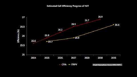
A significant milestone for HJT was LONGi achieving a world record efficiency of 26.81% for an HJT-only cell structure (i.e., not incorporating back contacts) in November 2022. This surpassed the long-standing record held by Kaneka (26.7% on an HBC structure, which combines HJT with Interdigitated Back Contacts). As for commercial efficiency, Huasun has been leading with mass production efficiency of 25.5% reached in 2023, 26.1% in mid-2024, and 26.5% by the end of last year. Emphasizing that the cell efficiencies are only for internal assessment purposes, companies have stopped talking about cell efficiencies, mostly promoting module power and efficiency. However, according to neutral sources such as CPIA, HJT cell efficiency was 25.4% in 2024, which improved by 0.3 percentage points to 25.7% in 2025 and is expected to reach 26.9% by 2030, which is 0.3 percentage points higher than TOPCon. On the other hand, ITRPV says the technology would only reach 25.7% in 2025, then 25.9% in 2027, and will take 10 years from now to reach 26.6% (see Low-Temperature HJT Manufacturing Adapts To Wider Wafer Variants).
HJT Processing
HJT has been promoted as a technology with fewer processing steps. After the silicon wafers are etched to remove saw damage and textured, intrinsic amorphous silicon layers are applied to both sides, followed by doped amorphous silicon films with opposite polarities. Next, a TCO film is applied to act as an antireflective coating and conductive electrode for current extraction. A metallic grid is then screen-printed on top of the TCO and cured to produce the HJT cell. While keeping these fundamentals intact, a few technical advancements in the HJT segment have driven the technology’s progress.
The Shift to Double-Sided Microcrystalline Silicon
A fundamental evolution within the HJT cell structure involves replacing the doped amorphous silicon (a-Si) layers with doped microcrystalline silicon layers. This transition has taken place sequentially: first replacing the doped a-Si layer on the emitter side (often referred to as HJT 2.0), and subsequently replacing the layer on the rear side as well, resulting in a double-sided microcrystalline structure (HJT 3.0). This architectural shift is motivated by the inherent material limitations of doped amorphous silicon. Compared to amorphous silicon, the microcrystalline silicon exhibits lower parasitic light absorption, particularly in the shorter wavelength range. This shift reduces the parasitic absorption losses of HJT to an extent.
Additionally, microcrystalline silicon has better electrical conductivity than amorphous silicon, which reduces series resistance losses within the cell, leading to an enhancement in the fill factor (FF). It also shares the responsibility for lateral conductivity with TCO to an extent.
The implementation of microcrystalline silicon layers requires advancements in deposition equipment and processes. All leading equipment vendors, such as Maxwell, have optimized their tool platforms, and these have been implemented at leading HJT makers. The structure has already been the standard for some time. The other important developments in the HJT segment are PIB-based edge sealants and the adoption of down-conversion encapsulation films as standard.
High Mobility TCO
A relatively more recent advancement in HJT processing is high-mobility target materials for TCO from Risen. The TCO layer is critical because it must balance 2 essential properties: high conductivity and high optical transparency. To optimize the TCO layer performance, Risen focused on 3 main directions: lowering the resistivity of the layer, increasing its light transmittance, and enabling low-temperature deposition for better compatibility with delicate cell structures, a few of which are counteracting. In practice, lowering the resistivity of the TCO layer is the primary goal. Resistivity largely depends on 2 factors: the carrier concentration and the carrier mobility within the layer. Increasing the carrier concentration can reduce resistivity, but it also increases light absorption within the TCO layer itself. This leads to less sunlight reaching the active cell area and ultimately reduces the overall cell efficiency. Conversely, improving carrier mobility reduces resistivity without negatively impacting light transmittance. Therefore, a careful balance between carrier concentration and carrier mobility must be achieved to optimize cell efficiency. Risen developed an optimized target material composition that enhances carrier mobility – a 29.11% improvement. This enhancement, while maintaining a favorable carrier concentration, led to an approximate 0.02% absolute efficiency gain at the single-cell level, according to Risen.
This text is an excerpt from the TaiyangNews Cell & Module Technology Trends 2025 report, which can be downloaded for free here.
