

TOPCon requires more demanding wet-chemical steps than PERC, including removal of thick BSG, rear-side PSG, and polysilicon wraparound
RENA promotes cluster-based solutions combining inline HF treatments with batch alkaline etching, supported by ozone cleaning and water-capping technology
SCHMID integrates single-side HF oxide removal with rear-side polishing and water masking, while Shenzhen S.C also promotes cluster approaches
When wafers move into the emitter formation stage after saw damage etching (SDE) and texturing, 2 unwanted outcomes typically occur: the formation of doped glass and the creation of an emitter on both sides of the wafer, as well as along the edges. These are typically removed again using wet-chemical processes. The process flow and tool setup at these wet-processing stations are highly sensitive to the cell technology being used. In SDE and texturing, the key difference between PERC and TOPCon lies in the base wafer polarity – p-type in PERC and n-type in TOPCon, which only requires adaptation at the end of the process, at least in principle. It is quite different in subsequent processes. For example, with TOPCon, the requirements are more complex. The BSG that forms on the emitter side is harder to remove than the PSG formed in PERC. Additionally, TOPCon processing also involves removing PSG from the rear side, as this area undergoes active diffusion to form the back surface field. In addition, TOPCon also requires the removal of polysilicon wraparound. While all these additional steps increase the complexity, they also create room for innovative approaches.
Cluster Etching Concepts & Full Inline-Based Concepts
Cluster Approach:
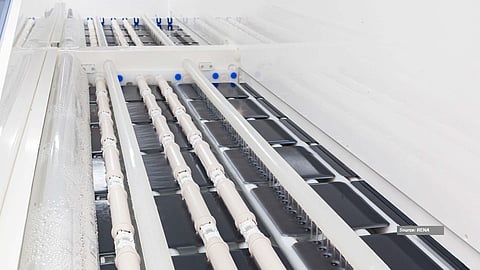
Inline processes have been adapted to meet these needs, and companies like RENA have developed cluster concepts. In the latter approach, wafers first undergo single-side HF treatment to remove BSG at the edges and rear, a task handled by inline tools. Since BSG is typically thicker and harder to etch than PSG, RENA has adjusted both HF concentration and temperature to enable a compact tool design while maintaining high throughput. With the front-side BSG acting as a natural mask, the wafers can then move into a batch system using alkaline etching with additives to polish the rear or remove poly wraparound on the front. The final step may include cleaning or further glass removal, depending on the process flow. To ensure uniform etching and process stability, the rear surface is first subjected to ozone oxidation, followed by etching and ozone-based cleaning. Other than RENA, Shenzhen S.C also promotes a cluster-based solution for these steps.
Inline Concept:
Alternatively, these etching steps can be handled entirely by inline tools. The specific chemistry and tool configuration depend on the layer being removed. All 3 companies with products listed in this category offer inline solutions as well.
RENA, while offering both approaches, mainly promotes its cluster-based solutions. The company tailors its process depending on the deposition method. According to Michael Vees, Sales Director Solar, RENA Technologies GmbH, the company recommends 2 clusters for PECVD and LPCVD processes – each combining inline and batch tools – with slight differences in the process sequence. These clusters are typically positioned before and after tunnel oxide and polysilicon deposition. For PVD processes, a single cluster is sufficient. When it comes to PSG removal after polysilicon deposition, Vees notes that only batch processing is required, as single-sided etching is not necessary. This setup provides manufacturers with the flexibility to meet various production needs.
Vees points out that BSG layers in TOPCon are typically 5 times thicker – about 130 nm – than in PERC, making them much harder to etch. Thus, achieving high throughput in a compact footprint is challenging. The key to efficient etching lies in balancing the concentration and temperature of HF. While a high concentration provides fast etching, it raises concerns about cost, safety, and waste management. A more balanced method uses medium HF concentration combined with elevated temperatures, which optimizes both etch rate and cost. As a rule of thumb, increasing the temperature by 20°C roughly doubles the etch rate. A third approach uses a relatively low HF concentration with an etch-rate-boosting additive and an elevated temperature. RENA has developed a solution using the third method, which employs an additive that is readily available, less toxic, and more economical than HF, it says. This approach not only saves costs but also improves safety and waste management, highlights RENA. These inline tools also feature water-capping technology, licensed from SCHMID, which enables precise single-side processing while protecting the front surface. For batch processes involving rear polishing, edge isolation, and poly wraparound removal, RENA promotes its Batch 3 N600 texturing platform.
SCHMID’s edge isolation solutions begin with inline single-side HF oxide removal, followed by rear-side polishing in a KOH bath at elevated temperatures. The front surface is protected by SCHMID’s patented water masking technology. By treating the wafer edges to be water-repellent, the system ensures the protective water layer on the emitter side stays in place, effectively shielding it from chemical exposure. The removal of doped glass that follows depends on the specific process design. The same system is also used for removing polysilicon wraparound and doped glass. The equipment features an advanced transport system within the cleaning modules that helps keep wafer surfaces clean. Process recipes are tailored based on the polysilicon deposition method and doping strategy. The sequence starts with HF preconditioning, followed by single-side poly etching, rinsing, and cleaning. Depending on the process flow, doped glass removal is achieved through HF immersion, after which the wafers undergo a final rinse and dry. The modular platform also supports a wide range of advanced solar cell technologies beyond TOPCon. For back-contact cells, where edge isolation must avoid damaging laser-doped areas, tool configurations increasingly incorporate masking and tailored chemical flows to enable precise rear-side polishing.
The text is an edited excerpt from TaiyangNews’ latest Market Survey on Solar Cell Production Equipment 2025, which can be downloaded for free here.
