
The sunny side of a standard silicon-based solar cell is pretty much set when compared to the rear side, which has become the focus of cell researchers, especially passivation. In fact, rear surface passivation is the key component of PERC type cell architecture, which is considered to be the next big thing in advancements at the cell level. No wonder the 2015 released International Technology Roadmap for Photovoltaic (ITRPV) discusses the important aspects of rear surface passivation. The 6th roadmap evaluates the materials of choice for rear surface passivation and different methods to deposit these dielectric films. Its takeaway: aluminum oxide deposited with Plasma Enhanced Chemical Vapor Deposition (PECVD) is and will be the predominant method.
Passivating the rear side
Here are some basics on rear-passivation before going into details: The main motivation for rear passivation is to reduce rear recombination losses. Application of aluminum back surface fields (Al-BSF) is the current state of the art for the rear side. This layer of aluminum applied with screen printing only provides a field effect passivation by shielding minority-charge carriers, but is is missing the chemical passivation part. The dangling silicon bonds on the rear surface also have to be passivated to reduce recombination losses from the back side. According to ITRPV's study, Al-BSF´s support cannot bring the rear recombination current values below 200 fA/cm2. To do so, an active dielectric passivation layer is required on the rear side, mimicking silicon nitride's job on the emitter.
Aluminum oxide dominates
Aluminum oxide has been a predominant material of choice as it fulfils all criteria for rear surface passivation. Its high fixed negative charge density enables it to provide an effective field effective passivation and at the same time it can also passivate silicon dangling bonds on the surface. However, according to the current roadmap, silicon oxynitride (SiONx) is also in the race. These dielectric films are often capped with silicon nitride. The reason for capping is that the rear passivation film is also held responsible for optical reflection on the back side, which requires thick layers of about 100 nm. Depositing such thick aluminum oxide film would not make economic sense. Thus, in order to makeup for the thickness required for optical reflection, the aluminum oxide film is capped with a less expensive silicon nitride film. The capping layer also protects the underlying passivation film from the possible damages arising from a high temperature firing process.
PECVD advantage
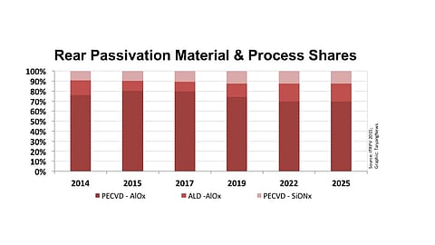
The method of deposition is yet another classification criterion. The choice here is between the very old companion of PV, PECVD, and relatively new, but quality oriented Atomic Layer Deposition (ALD). Nearly every PECVD based silicon nitride deposition system supplier offers tools that support aluminum oxide deposition. While ALD is widely used in semiconductor manufacturing, several equipment makers have developed solar-specific product platforms. According to the roadmap, PECVD deposited aluminum oxide will retain its dominance with 80% market share till 2017 and would slip only by about 10% over the next 10 years. ALD deposited aluminum oxide is expected to be the main beneficiary of this fall, increasing its presence from 10% to about 18%. However, those who want to opt for silicon oxynitride have no other choice than PECVD for deposition. The roadmap estimates a 10% presence for this rear passivation material and expects no considerable growth in the coming 10 years.
Irrespective of the deposition technology and films composition, PECVD is commonly employed for applying the capping layer. Thus opting for the same machine to apply also aluminum oxide offers a better synchronization at the tool level. In addition, the PECVD process inherently supports a higher throughput over its rival ALD. But films deposited with ALD have a higher quality. Here, the films are grown layer by layer at the atomic level, resulting in a good step coverage. And due to its superior quality, ALD can deposit relatively thin films that are sufficient to realize the desired levels of passivation. At the end it is simply a choice between, quality, cost and complexity.
