
Key takeaways:
Fraunhofer ISE’s new lab provides infrastructure to bridge lab-scale research and industrial manufacturing
It will play a key role in scaling up perovskite-silicon tandem technology as it approaches early commercialization
The facility supports multiple deposition and coating processes aimed at improving stability, throughput, and efficiency
Perovskite-silicon tandem technology is considered next-generation PV technology, and is in the early stages of reaching commercial-scale production. This technology is expected to start commercialization in the next 3 to 5 years, according to panel speakers at the recent TaiyangNews Next Generation PV Technology Conference. Perovskite, when used in tandem with silicon, can increase the cell’s efficiency potential. However, there are also challenges to scaling this technology.
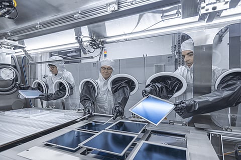
To accelerate the market readiness of perovskite-silicon tandem technology, Fraunhofer ISE recently established a lab platform called Pero-Si-SCALE. This facility offers equipment, cell, and material manufacturers a platform to test and develop their products. The lab supports its customers in selecting equipment for prototype and pilot manufacturing, and in transferring the process know-how. The already established research departments of Fraunhofer ISE – PV-TEC for cells and Module-TEC for modules – are also integrated with the Pero-Si-SCALE project. This platform enables evaluation of the entire process chain, from materials to modules, for this technology.
The laboratory services include scalability of vapor deposition processes for large-area tandem cells. It uses high-rate linear evaporators to deposit contact layers such as C60 and to co-evaporate perovskite absorbers. Industrial sputtering and atomic layer deposition (ALD) of various metal oxides, dielectric layers, buffer layers, and ultra-thin passivation layers across a wide range of materials are also possible, and are designed for up to G12 wafer size.
Pero-Si-SCALE facilitates the manufacturing of tandem cells using traditional wet-chemical processes to deposit perovskite, contact, and passivation layers. In addition, the facility also includes dip and spray coating, and scalable printing technologies such as inkjet, rotary, and slot-die printing. The infrastructure also includes a high-precision annealing process in a controlled atmosphere for the crystallization of the perovskite layer. Several other processes in perovskite-tandem cell fabrication are evaluated and optimized at this facility to achieve deposited layers with high stability and purity and high-quality final cells.
By offering these processes, optimization, and technology developments, the Pero-Si-SCALE aims to evaluate the entire perovskite-silicon tandem cell manufacturing process and scaling. It also focuses on comprehensive characterization with an ultimate goal of improving process stability, throughput, and efficiency.
Dr. Ralf Preu, Head of the Photovoltaics Division at Fraunhofer ISE, said, “The new laboratory infrastructure builds on 20 years of experience in industry-oriented development of silicon photovoltaics at the Photovoltaic Technology Evaluation Center (PV-TEC).” He added that the PV-TEC center can also ensure the supply of optimized silicon bottom cells to the lab’s ecosystem for the ongoing research and development of tandem cells.

