

Key takeaways:
Indium reduction and indium-free TCOs are emerging as important long-term development targets for HJT
Alternative deposition approaches, such as hot-wire CVD, are being explored to lower equipment costs and increase throughput
Existing HJT production equipment may find broader applications, including use in certain BC manufacturing processes
Besides silver consumption, heterojunction (HJT) manufacturing has another material that could pose a challenge: indium, used in transparent conductive oxide (TCO).
At the TaiyangNews High-Efficiency Solar Technologies 2025 Conference, Huasun’s Christian Comes said that indium is not yet a critical bottleneck at today’s production scale of 40 GW, but it could become one if HJT expands much further, for example, 200 GW. The company is therefore already reducing its use of indium and has an indium-free solution ready for the future. 3SUN also pointed to indium-free TCO as an important development route.
Risen, on the other hand, exclusively addressed rear-side TCO challenges. The company has engineered a stack of materials to achieve a sheet resistance greater than 80 Ω/sq while maintaining IR transmittance. Po-Chuan Yang, Dean of Global Photovoltaic Research Institute at Risen Energy, also highlighted that combining the high-mobility TCO of over 120 cm²/Vs with 18 μm fingers could further boost cell efficiency by increasing the fill factor and short-circuit current. Meanwhile, the company continues to focus on indium-free targets to reduce costs.
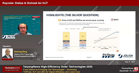
On the CapEx side, hot-wire CVD (HWCVD) could be a potential alternative to PECVD as part of cost-reduction efforts. Forschungszentrum’s Kaining Ding emphasized that the technology enables wafer processing on both sides, which could effectively double the throughput. In addition, the equipment is simpler, as it does not rely on plasma, making it inherently lower cost. However, development in this area remains limited. Only a few equipment suppliers, mainly in China, are working on HWCVD, with activity largely confined to pilot lines. There has been an attempt to scale up to a 1 GW system, but it is currently on pause, mainly due to the recession. The main challenges remain throughput and scalability, which are yet to be fully resolved.
Another point raised by Ding relates to equipment CapEx and utilization. Traditionally, HJT has been seen as a standalone technology with a distinct process flow, requiring dedicated equipment not shared with other cell architectures. However, this is now beginning to change. In its latest BC architecture, LONGi uses an HJT-based structure for the p-side. According to Ding, the company has retrofitted existing HJT equipment to deposit the intrinsic and p-type layers as well as the TCO films. This development expands the scope of applications for HJT production lines. In practical terms, at least part of an HJT line can now be repurposed for HIBC manufacturing if the manufacturer has this BC technology in the roadmap.
The text is an edited excerpt from TaiyangNews’ report on Cell & Module Technology Trends 2026, which can be downloaded for free here.
