

Wafer thinning is a priority across the crystalline-silicon value chain, but remains challenging at ultra-thin scales
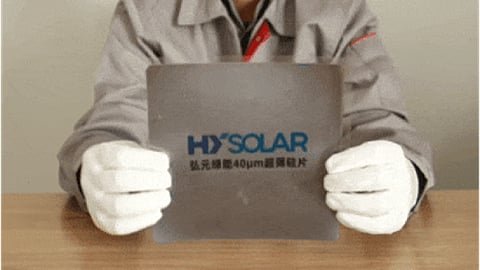
HY SOLAR has produced 40 μm ultra-thin monocrystalline wafers in full-size and half-cut formats at its Baotou facility
The production run supports manufacturing feasibility for ultra-thin wafers using in-house slicing equipment
Wafer thinning has become a key focus across the crystalline-silicon value chain. The photovoltaic (PV) industry is seeking to reduce material consumption and manufacturing costs. Thinner wafers improve material efficiency and enable lighter and more flexible PV applications. However, stable manufacturing at ultra-thin form factors remains challenging. Key issues in this process include wafer breakage, stress control, and yield losses during slicing and downstream processing.
Chinese wafer manufacturer HY SOLAR reported producing 40 μm ultra-thin monocrystalline silicon wafers. The wafers were produced using internally developed slicing equipment at the company’s intelligent wafer manufacturing facility in Baotou, Inner Mongolia. The production run included both full-size and half-cut formats. According to the company, the wafers meet key mechanical and dimensional requirements for ultra-thin substrates.
Producing wafers at thicknesses below current commercial levels requires tight control over stress, wire stability, and cutting precision. HY SOLAR stated that its approach combines equipment- and process-level optimization. This includes compact structural design, low-tension wire control, and the use of fine diamond wire with reduced groove spacing to reduce kerf loss.
Additional process measures focus on reducing wire vibration and stabilizing stress. HY SOLAR also mentioned its efforts to mitigate micro-crack formation during slicing. These measures are applied while maintaining compatibility with both full-size and half-cut wafer processing.
The slicing platform integrates online monitoring and feedback systems. These systems support stable operation across different wafer sizes and thicknesses. Core components such as guide wheels, spindle systems, and control modules are developed and controlled internally. This supports closer alignment between equipment operation and process requirements.
According to the company, the ultra-thin monocrystalline wafers exhibit controlled oxygen and carbon content. The wafers also show uniform resistivity and high minority-carrier lifetime. These material properties are relevant for multiple cell architectures. However, the company didn’t disclose downstream cell performance data. HY SOLAR also noted that its wafer products have obtained carbon footprint certification under the French ECS framework.
TaiyangNews is bringing together the Indian solar PV manufacturing industry for the Solar Technology Conference India 2026 (STC.I 2026). To be held on February 5 and 6 in Aerocity, New Delhi, this 2nd edition of the TaiyangNews physical conference will also have banks, investors, and policymakers in attendance. Register for the event here.
