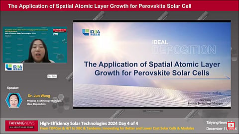

Ideal Deposition's SALD tool offers shorter processing time compared to conventional sequential ALD technology
SALD technology is suitable for large-area substrates
The tool maker offers 3 types of SALD tools – R&D scale, pilot line, and mass-scale – for the perovskite cell fabrication process
The Atomic Layer Deposition (ALD) tool is widely used in the industry, particularly for depositing atomic-level, dense, pinhole-free, and conformal thin films, such as Al2O3 for surface passivation on silicon solar cells. However, the conventional sequential ALD technique is limited by slower deposition rates. In contrast, the Spatial Atomic Layer Deposition (SALD) tool overcomes this limitation, allowing for faster deposition rates of several nanometers (nm) per second.
In this context, Dr. Jun Wang, Process Technology Manager at Ideal Deposition, a Chinese manufacturer of PV cell production tools, provided a brief overview of the company’s SALD tool, suitable for perovskite cell production, at the TaiyangNews Annual Flagship Conference – High-Efficiency Solar Technologies 2024 (see Ideal Deposition presentation here). Founded in 2013, the company has primarily focused on manufacturing solar cell production tools, including diffusion tools, annealing, and oxidation equipment. Currently, its production capacity has reached 400 units per year, according to Wang.
The ALD deposition process enables the growth of dense, pinhole-free, and conformal thin film layers at the atomic level through the sequential exposure of the substrate to precursors. In this layer-by-layer growth, the precursor gas first reaches the substrate, followed by an inert gas. The second precursor gas then reacts with the first precursor, which has been absorbed by the substrate, completing the deposition cycle. These substrate reactions are self-limiting, yielding one monolayer per cycle. The purging steps prevent the mixing of the precursors, which would otherwise reduce the uniformity of the deposition. The deposition cycle is repeated until the desired number of layers is attained, as explained by Wang. Although ALD deposition technology is widely acknowledged for its ability to deposit high-quality layers on silicon PV as well as on perovskite cells, the long process steps severely limit its throughput.
A variant of ALD, SALD features spatial rather than temporal separation of precursors, eliminating the need for purge steps and increasing the deposition rate compared to ALD. In the SALD process, both the precursor and the inert gas continuously flow toward the substrate, moving laterally relative to the shower height through multiple channels. Meanwhile, the introduction of the inert gas between the precursors acts as a barrier that prevents precursor intermixing and directs the precursor molecules toward the exhaust. Following the proper separation of precursors, which only react with the substrate or previously deposited layers in a layer-by-layer manner, the final deposition occurs, as stated by Wang.
The company offers 3 types of SALD tools: R&D level, pilot level, and mass-production level. These tools, suitable for substrates such as glass, silicon, and flexible materials, can deposit thin films of SnOx, AlOx, ZnOx, and NiOx, with deposition temperatures ranging from 80°C to 300°C. According to Wang, the R&D-level tool, compatible with substrate sizes up to 300 x 400 mm, can deposit a 20 nm thick coating with a nonuniformity of less than 3% in under 18 minutes per cycle. For pilot line and mass-production level tools, the maximum coating size can reach approximately 1.2 x 2.4 m, with a nonuniformity of less than 5%, added Wang.
Ideal Deposition’s SALD tool is equipped with a loading/unloading mechanism, load-lock-in (LLI), pre-heating chamber, process chamber, and load-lock-out (LLO) mechanism. This LLI and LLO process chamber serves as a barrier between the external atmospheric pressure and the vacuum pressure inside the tool.
Regarding the quality of SALD tin oxide (SnOx) layer deposition for perovskite cell applications, the film thickness increases with the number of deposition cycles, at a growth per cycle (GPC) rate of 0.1 nm/cycle, according to internal data from Ideal Deposition. This SALD SnOx layer, with a thickness of 20 nm, can deliver up to 96% transmittance while effectively preventing water permeation. Furthermore, the deposition of SnOx over large areas of Si and glass demonstrated good thickness uniformity and a refractive index of approximately 1.9. Similarly, the SALD-deposited AlOx layer exhibited good thickness uniformity (2%) and a refractive index of 1.62, according to internal test data.
