

Ozone-based wet processing can cut chemical and water consumption significantly, according to RENA
While the key focus for Leadmicro was edge passivation solution, S.C New Energy presented the competitive advantages of PECVD
Fine-line printing and silver reduction strategies – especially nickel blending and copper-based pastes – are key to balancing efficiency gains with cost reduction, according to Solamet
Lasers are becoming central to cell processing, enabling efficiency gains through poly-finger formation, edge defect mitigation, and advanced patterning
WAVELABS highlighted that LED-based characterization platforms integrate multiple measurements with high precision and support next-gen cell formats
Utilities, though in the background, dominate lifetime costs; optimized OpEx and turnkey solutions are critical to avoid delays and ensure fab profitability, according to UHP
Indian solar manufacturing is taking a first, but massive, step toward true vertical integration. With the implementation of the ALCM (ALMM-II) mandate, which is due very soon, module makers and downstream players are increasingly venturing into large-scale cell production. While this shift is currently policy-driven, it fundamentally addresses the long-term goals of supply chain security and technology sovereignty. Once the technology has been narrowed down, the immediate requirements for establishing cell fabs are selecting production equipment and securing material supply. These 2 pillars of the manufacturing ecosystem govern the critical performance indicators of a fab: efficiency, yield, and cost.
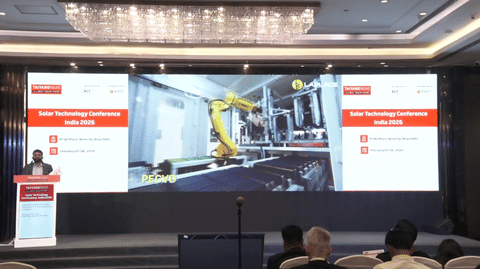
Against this backdrop, the session on cell production equipment and materials at the TaiyangNews Solar Technology Conference India (STC.I) 2026, a physical event held in New Delhi in late February 2026, provided a timely and comprehensive overview of solutions from leading equipment vendors. The session also included inputs from materials and fab utilities, including power, water, air, gases, and chemical supply and treatment infrastructure. Given the breadth of the topic, the session was conducted in 2 parts. This summary follows the sequence of presentations as delivered at the event. These include wet processing, deposition, metallization, laser systems, characterization, and the essential utilities required to support advanced cell manufacturing.
Indian Manufacturers’ Perspective
Setting up the scene, Rajiv Arya, Technology Vice President at Indian manufacturer Jakson Solar, shared the manufacturer's perspective. The choice of technology is the first step towards building a manufacturing base. Jakson’s technology assessment concluded that TOPCon remains the most viable near-term cell technology for Indian manufacturers despite the industry’s rapid evolution toward back-contact (BC) and tandem concepts. The technology is expected to remain the dominant mainstream platform for quite some time, Arya estimates.
He noted that one of the main concerns for new investors is the risk of technology obsolescence, i.e., whether a newly installed line can remain competitive if next-generation technologies are commercialized shortly after commissioning. One such protective measure is incorporating an optional edge passivation deposition capability in parts of its line. The company plans to maintain both EPD and non-EPD process options initially, allowing later expansion as the technology matures.
Emphasizing the challenges to the expansion of Indian cell manufacturing, Arya notes that India still lacks domestic capability across critical parts of the upstream value chain, including wafers, polysilicon, specialty gases, consumables, and spare parts. As a result, manufacturers remain heavily dependent on imported equipment, technology, and raw materials. This dependence not only increases logistics and supply chain costs but also limits India’s ability to fully localize solar manufacturing economics. Arya further highlighted high capital expenditure (CapEx) and financing costs as key barriers to new cell investments. Compared with other manufacturing hubs, India faces higher equipment costs, more expensive financing, and longer payback periods, complicating project economics for investors.
Execution timelines also remain significantly longer than in China. While some Chinese manufacturers reportedly complete cell plant setup in as little as 6 months, Arya said Indian projects typically require about 1 year from concept to commissioning, even with optimized execution. Another major bottleneck is the shortage of skilled manpower. While labor availability is not a concern, Arya said India still lacks sufficient skilled manpower for advanced process-driven manufacturing such as solar cells. Overall, Arya said India’s cell manufacturing sector remains in an early learning phase, with companies still building process expertise while simultaneously navigating rapidly changing technology roadmaps.
CapEx and OpEx Optimized Solutions
Moving into the core of the session, the discussion began with updates on wet-chemical processes – the first step in the cell manufacturing sequence. Damian Brunner, Senior R&D Manager at the wet-chemical solutions expert RENA Technologies, elaborated on advanced wet-processing strategies for TOPCon manufacturing. Brunner utilized a series of relatable analogies to illustrate the importance of balancing CapEx with operational expenditure (OpEx) and reliability in industrial solar production. He compared low-cost equipment to budget consumer goods, noting that while they may save money upfront, they often lead to ‘unscheduled vacations’ (downtime) and higher long-term costs. The company offers 2 distinct tracks: one is OpEx-optimized, focused on the lowest possible running costs and maximum long-term reliability, while the other is CapEx-optimized.
As part of its low OpEx solutions for inline processes, such as single-side glass/oxide etching, the company offers the InEtchSide 4 and InEtchSide 4+ series wet processing tools. These tools, with a maximum single-sided etching speed of 5 m/minute, can reach up to 17,500 wafers/hour. To support this throughput as well as to protect the optical yield, the wafers are provided with water capping protection.
For the other processes, namely texturing, edge isolation, and removal of Poly-Si wraparound, the company offers its Batch 3 N600 platform. Brunner highlighted that the solution features ozone-based pre- and post-cleaning, water- and waste-saving technologies that are key drivers of OpEx reduction, with ozone-based cleaning as the key driver.
RENA’s ozone-based cleaning technology, which significantly reduces the need for expensive chemicals such as KOH and H2O2, can lower total ownership costs by up to 40% compared to traditional pSC1 processes (part of RCA clean). Addressing India's environmental mandates, Brunner showcased WaterSaving 1.0 technology, which currently cuts water consumption by 50%, with a roadmap to reach 70% savings in the near future.
Complementing this OpEx-friendly tool, Brunner presented the company’s lower-CapEx alternative without ozone-based cleaning and optional water-saving technology, for clients with budget constraints.
Edge Passivation in Focus
In his presentation, Baochen Liao, CTO of Leadmicro, provided a comprehensive overview of the evolution of TOPCon into the next generation. The key elements of this evolution, which Liao refers to as TOPCon 4.0, are rear poly-fingers, edge passivation, and stencil printing at the cell level and multi-cut layout at the module level. Limiting the scope of this presentation to solutions offered by Leadmicro, Liao presented details on rear poly-fingers and, more importantly, edge passivation, along with the details of the associated equipment.
Lasers figure at the top of the list, which are increasingly finding applications in solar cell processing. For TOPCon, lasers, in addition to their use for known applications such as cell slicing and contact firing, are also key to realizing poly-thinning in rear poly-finger technology. Lasers also have a similar application in BC – patterning – which is the most critical for the architecture. Leadmicro has developed laser solutions for all these applications. The key aspects of lasers are output power, spot roundness, and shaping uniformity, emphasizes Liao.
The next and, in fact, the key topic of Liao’s presentation was edge passivation. The extent of damage to the slice edge highly depends on laser separation. Nevertheless, Liao emphasizes that laser separation introduces defects such as melting, stress, dislocations, and dangling bonds. These defects lead to non-uniform surfaces and increased recombination, particularly near the p-n junction.
To address the diverse nature of edge damage, Leadmicro offers edge passivation tools based on aluminum oxide deposition. Liao emphasized that the company’s solutions are designed with a strong focus on ‘one-stop’ applicability. That means the tool platform is compatible across multiple cell architectures, including TOPCon, BC, and advanced designs such as 0BB and poly-finger structures. In addition, the equipment supports various cell formats, cell-slicing configurations from half-cut to third- and quarter-cut cells, as well as different wafer sizes, such as M10, G12, and rectangular formats. This modularity makes the tool CapEx-effective in the long run, according to Liao.
On the process front, the company’s tool platform facilitates all passivation mechanisms. Its edge passivation system is based on a tube-type ALD configuration, which, according to Liao, results in high-density films that provide better chemical passivation. The high, fixed negative of aluminum oxide generally provides field-effect passivation. The hydroxyl treatment, which is part of the ALD half-reaction, facilitates interface treatment as part of hydrogen passivation. Thermal treatment and light soaking are also integral parts of the process. It also results in conformal coating on uneven surfaces.
Another important feature of these edge passivation tools is their remarkably high throughput, which makes a business case even under the prevailing overcapacity conditions. Leadmicro’s edge passivation tool supports a throughput of 20,000 pieces per hour, irrespective of size and configuration. The resulting passivation quality is reflected as achieved lifetimes exceeding 760 µs and thickness uniformity within ~3%.
PECVD is Preferred – S.C New Energy
The conference also featured input from another leading equipment supplier, S.C New Energy. Homer Chen focused on comparing different deposition technologies, particularly PECVD and LPCVD. He noted that the company’s customers show a clear preference for PECVD, with an adoption ratio of about 2.2:1. This higher uptake is attributed to advantages such as higher throughput, longer process tube lifetime, in-situ doping capability, and improved film uniformity. According to Chen, major TOPCon manufacturers, including Tongwei, Trinasolar, Solarspace, and JA Solar, either use both PECVD and LPCVD processes or rely solely on PECVD. Based on mass production data, Chen stated that PECVD-based process groups exhibit better efficiency distribution once cell efficiencies exceed around 25.3%. In addition, key performance indicators such as yield, peak efficiency, and breakage rate also favor PECVD over LPCVD.
On the quality control side, Chen highlighted that the company offers solutions for both plate-type and tube-type vacuum coating systems. Its laser ablation-based cleaning technology removes residual films from trays in plate-type tools, while dedicated solutions are available for cleaning graphite boats in tube-type systems. These approaches support stable mass production and enable in-house maintenance. He also noted that real-time monitoring of process gas composition in the reactive plasma deposition (RPD) chamber is possible with optical emission spectroscopy (OES), reducing the need for offline inspection of parameters such as film thickness, sheet resistance, and transmittance.
Chen added that S.C New Energy’s TOPCon production lines – covering wet processing, deposition, and factory automation – are protected by proprietary intellectual property.
Insights into Metallization
Metallization remains a critical process affecting both cost and performance. The pastes, especially, are also very sensitive to any process or structural changes. Daniel Lim of Solamet presented an overview of the latest developments in the most expensive process consumables for cell lines – pastes. A key theme of the presentation was fine-line printing. In this context, stencil-based fine-line metallization is emerging as a key development for TOPCon. Enabling narrower finger widths of about 9 µm with higher aspect ratios, achieved with 7 µm-height stencil printing, improves line morphology, thereby supporting better current collection while reducing shading losses. This approach, however, requires dedicated paste formulations that combine optimized silver powder with tailored organic systems to ensure stable and high-quality printing. Compared with high-mesh screen printing, stencil printing with an increased finger count shows a reduction in paste laydown of about 1 mg, according to Lim.
As part of the solutions for fine-line printing, Lim also discussed laser-transfer printing. By transferring 10 µm films, the technique enables well-defined finger geometries with high aspect ratios. On the performance front, this supports reduced shading and improved current collection, as reflected in an absolute efficiency gain of around 0.13%. At the same time, the technology is still undergoing optimization. Key challenges include micro-breaks of 50 µm that are difficult to detect during visual inspection. The higher aspect ratio of the fingers also introduces the risk of finger peeling during downstream post-firing processes. In addition, achieving finer trench dimensions requires higher laser power, which can, in turn, lead to paste splattering and negatively affect current collection.
Emerging approaches such as stencil printing and laser transfer were identified as next-generation solutions that require significant paste customization to match evolving cell designs, including poly-finger architectures. These approaches enable narrower finger widths, delivering efficiency gains and material savings, with reported improvements of around 0.1% to 0.2%. However, challenges remain in paste contact formation and process integration, especially as front-side designs become more complex. Lim also highlighted the interaction between metallization and passivation processes, noting that certain passivation treatments can degrade paste performance, necessitating tailored formulations.
On cost reduction, Solamet outlined multiple pathways to reduce reliance on silver, which remains a major cost driver. These include lowering paste solid content and introducing metal blending. An interesting development here is that nickel is found to offer better stability than copper for fine-line printing. For example, 10% nickel blending or a reduced silver content can maintain a comparable level of efficiency, according to Lim. The company is also advancing toward lower silver fractions, targeting as low as 10% silver content in copper-based pastes, while addressing reliability challenges such as adhesion and oxidation.
Looking further ahead, the complete transition to copper-based metallization offers the highest cost-saving potential but introduces greater process complexity, including multi-step printing and differing sintering conditions.
Ever-Increasing Applications for Lasers
Lasers are increasingly being used in solar cell processing. Reflecting this trend, the cell production equipment session at STC.I 2026 featured DR Laser, a market leader in the segment. Ravinder Bhardwaj, VP Sales & Business Development at NMTronics, DR Laser’s Indian partner, presented the latest product portfolio. The solutions are primarily aligned with the 2 dominant cell technologies – BC and TOPCon.
On the TOPCon side, the company offers tools for a wide range of processes, including laser-enhanced contact optimization (LECO), half-cell edge passivation, poly-Si finger, and metallization line. For the TOPCon rear poly-finger, which requires laser-based rear selective tunneling contact, Bhardwaj introduced the latest TCP series tool. Featuring 4 laser sources, this tool offers a throughput of up to 9,600 wafers per hour for M10-size wafers. The tool is a key enabler for realizing an efficiency gain of 0.1% to 0.15% with poly-finger technology. Bhardwaj presented results for TOPCon cells with a rear poly-finger structure processed using DR Laser’s tool, achieving an absolute efficiency gain of 0.1% to 0.15% and 3 to 5% higher bifaciality. The latter results from reduced parasitic absorption in the rear-side polysilicon film due to thinning. Bhardwaj further noted that the attributes of these efficiency gains vary depending on the Poly-Si deposition route, PECVD, or LPCVD.
The presentation also included another innovative application of lasers to reduce damage at the sliced edges. In addition to optimizing laser parameters for cutting, lasers can also be used to selectively remove the emitter at the laser-cut positions. The step circumvents the most pronounced defect of the cut, which is at the junction area. The solution can work independently and complement edge passivation. Following this approach, the emitter is removed locally immediately after its formation. DR Laser calls its tool TCI, which has a throughput of up to 9,000 wafers/hour. The company characterizes this solution as the most cost-effective edge passivation approach, especially when compared to edge passivation deposition tools.
DR Laser has also entered the business of supplying metallization equipment by launching a full metallization line in 2025. The solution consists of pattern transfer printing (PTP), screen printing, laser-induced firing, and tester & sorter. The PTP, which the laser tool maker has been developing for the last 1 year, is capable of achieving finger widths of 10 μm and the same height, resulting in an aspect ratio of 1. The thickness uniformity of the fingers is ±2 μm. Needless to mention, lasers are critical for realizing patterning in BC cell processing. The key features here are large-spot ablation, fine-tuning of the patterning, and flexible optimization of laser ablation. DR Laser also offers laser-based soldering tools for the BC module.
LED-Based Characterization For Advanced Cell Manufacturing
As cell architectures continue to evolve, characterization tools must adapt to both incremental and breakthrough changes. Covering this aspect, the Director of WAVELABS Eternal Sun, Samuel Raj, presented the company’s LED-based tools, targeting mass-scale production. The key attribute of WAVELABS’ products is their use of an LED light engine. Compared to conventional xenon sources, the LED spectrum matches the target wavelength within ±5%, with deviations controlled to below 3%. Integrated with a spectrometer, the system enables spectrally controlled and intensity-corrected measurements, achieving a module-level power measurement uncertainty of just 0.9% at STC.
Beyond standard IV and power measurements, the tools integrate multiple characterization functions into a single platform, reducing the need for offline inspections. These include multi-cut and ZBB cell measurements using multi-channel and multi-probe configurations. With an illumination area of 260 × 260 mm, the system supports large wafer formats such as M12R, M12, and G13 without compromising cycle time. Additional selectable features include Suns-Voc for resistive-loss analysis, base doping for wafer-resistivity profiling, EQE for optical performance, PL and EL imaging, and grid resistance for metallization-quality assessment.
For process optimization and ramp-up, the tools provide real-time data accessible via SQL-based servers or MES systems. The Factory View function further enables centralized monitoring and analysis across multiple tools within a production line.
For tandem applications, the integrated spectrometer enables automatic calibration of the top and bottom cells in 200 ms, supporting mass-scale Si-tandem characterization. The LED light source also offers a long operational lifetime without compromising spectral stability.
Updates on the Utilities Front
All the solutions discussed so far fall under front-end processing, while utilities – though less visible – are equally critical for ensuring smooth and efficient production. Manjunath Jyothinagara, Managing Director of UHP Technologies, shared the importance of turnkey utilities and how to optimize project cost overrun. The key focus of his presentation was utilities' CapEx vs. OpEx, and he mainly advocates for the latter over the former.
Jyothinagara set the context by saying, “CapEx is one-time, but OpEx is going to be lifetime.” Using a 2.4 GW cell line as a reference, he compared process tools and utilities across parameters such as CapEx, manpower, land, and electricity, highlighting that even minor changes in byproducts like exhaust can significantly increase cooling, water, and power requirements. This underscores the need to carefully evaluate utility design and not to be lured by lower upfront costs.
Jyothinagara advocated for turnkey utility solutions over fragmented sourcing, citing benefits such as reduced coordination, streamlined project execution, and simplified operations. Addressing project delays – often caused by design integration and execution gaps – he estimated opportunity losses of up to ₹570 crore for a 4 GW project. To mitigate such risks, he proposed a hybrid model combining rental and capital assets in a 40:60 ratio. This enables faster project deployment. While the approach may increase OpEx, the resulting reduction in delays and quicker revenue realization can offset the additional costs. He positioned UHP Technologies as a value-chain partner supporting CapEx planning, rental solutions, OpEx optimization, and long-term operations and maintenance.
