

SDE remains essential despite earlier efforts to eliminate it, as finer pyramid structures and residual wafer roughness demand stable surface preparation
SCHMID’s Rainbox inline system enables precise front-side alkaline texturing for TOPCon, maintaining rear-side integrity and uniform reflectance below 12%
Larger wafer formats are impacting wet-bench design, requiring adjustments in bath sizes, carrier designs, including inline lane configurations
In our previous article, Texturing - A Key Surface Preparation Step In Solar Cell Manufacturing, we discussed chemistry, pyramid structures, and additives. We now discuss inline solutions, throughput challenges, and wafer format evolution. These aspects are becoming increasingly important as cell architectures advance. RENA is also working on wet chemistry to address the future needs by developing solutions for next-generation perovskite-silicon tandem technology. The company calls it nanotexturing, which aims to create pyramid structures with sizes around 500 nm to facilitate better light management and absorption. The potential elimination of SDE, which was one of the highlights in earlier surveys, appears to have gone out of trend. According to Gerry Knoch, Managing Director of exateq, completely removing SDE from the process remains unlikely, given the surface requirements of today’s high-efficiency cell architectures. The shift toward smaller pyramid structures – down to 1.5 μm – has made surface roughness even more critical. While the industry’s transition from slurry to diamond wire cutting has improved wafer quality, residual roughness at such fine scales still poses challenges. As a result, SDE remains an essential step for achieving uniform and effective texturing. Even RENA, which had been working towards eliminating SDE, continues to offer SDE as part of its texturing tools.
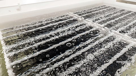
While neither a trend nor new, SCHMID’s inline solutions using alkaline chemistry deserve special mention here. This selective front-side treatment is especially valuable for technologies like TOPCon, where maintaining rear-side integrity is crucial for both optical and electrical performance. The system features a patented non-pressurized spray system, known as Rainbox, which applies a heated chemical solution to the wafer surface. Each Rainbox unit delivers fresh chemistry to achieve the desired pyramid texture. The process sequence includes pre-cleaning, alkaline texturing using a KOH solution at elevated temperatures, followed by a series of rinsing steps, metal and ozone cleaning, and final rinsing and drying. The operation temperature typically ranges from 60 to 80°C, depending on the additive. The main process consumables are KOH and deionized water. This method removes about 4 to 5 μm of silicon from the wafer surface and achieves a reflectance of less than 12% across the 400 to 1,000 nm wavelength range and below 9% at 600 nm. It also provides texture uniformity across and between wafers.
Throughput is a key metric of equipment performance, and exateq’s Knoch highlights the main challenges on this front. As wafers become larger and thinner, they also become more flexible, which can lead to handling issues. When the shift toward G12 wafers began in China, manufacturers initially had to increase the pitch between wafer slots. This meant either sticking with the existing bath size and accepting lower throughput or enlarging the bath to maintain capacity. According to Knoch, Chinese manufacturers chose to increase bath sizes, while non-Chinese manufacturers kept standard bath dimensions and accepted a slight reduction in throughput. However, this does not seem to hold true today. Much like other PV equipment makers, wet-bench suppliers are now offering GW-scale tool platforms that enable a single system to support gigawatt-level production (see Surface Processing For TOPCon, HJT & BC Solar Cells).
When discussing capacities, wafer size naturally comes into focus. Wafer formats continue to evolve as manufacturers seek larger sizes to enhance module power and efficiency. As Michael Vees, Sales Director Solar, RENA Technologies GmbH, noted that the industry quickly moved from debating M10 (182 mm) and G12 (210 mm) wafers to the widespread use of G12 half-cut wafers, particularly in HJT. exateq confirms that G12 half-cells are currently the most favored size, followed by G10 half-cells, although G10 full-size wafers still hold a noticeable share. G12 full-size wafers, on the other hand, represent only a minor portion of production, though some manufacturers continue to use them. For TOPCon, the industry has largely adopted rectangular cell formats. However, the impact on wet benches with this shift is minimal, since rectangular cells are typically produced by slicing fully processed cells. More recently, HJT suppliers have also started adopting rectangular formats. Perhaps the most surprising development with respect to wafer formats is that the pursuit of larger wafers hasn’t stopped at G12. Both RENA and exateq underscore receiving inquiries for G13 wafers with a 230 mm side length, with RENA noting that interest emerged as early as mid-2023. Wafer size evolution does affect wet benches, particularly for batch processes, which require new carrier designs. Inline systems are not immune either – for example, an inline tool designed with 12 lanes for M10 wafers must be downsized to 10 lanes when optimized for G12.
The text is an edited excerpt from TaiyangNews’ latest Market Survey on Solar Cell Production Equipment 2025, which can be downloaded for free here.
TaiyangNews hosts 2 upcoming conferences in September: the Cell & Module Production Equipment & Processing Materials Conference on September 2, 2025, free registration here, and Solar Made in the USA on September 8, 2025, in Las Vegas: register via RE+ here.
