
Key takeaways:
Linton's portfolio covers the complete silicon wafer manufacturing chain
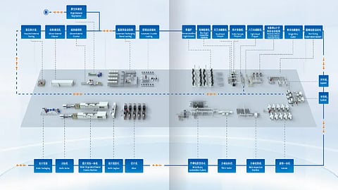
The production line combines automated ingot machining with intelligent diamond wire slicing and defect inspection
The company also showcased a low-oxygen crystal growth solution and process packages for advanced n-type cell technologies
Linton Technologies, an upstream PV manufacturer based in China, showcased its latest ingot and wafer production offerings at SNEC 2026.
The product portfolio included not only products but process solutions for the mainstream and high-efficiency cell technologies, such as TOPCon, back-contact (BC), and heterojunction (HJT).
Similar to other wafer-slicing equipment providers, Linton also offers intelligent, integrated solutions that combine its individual equipment into a single system, right from slicing the head and tail of an ingot to squaring, grinding, and wafer slicing.
For the first step, the company offers an automatic cut-off machine that is complemented by AGV loading, automatic tool alignment, sample wafer collection, head and tail cap removal, and ingot unloading. With fully unmanned operation, the tool's production capacity exceeds 1.5 GW, according to the company.
For squaring ingots, Linton’s tool can accommodate ingots up to 385 mm in diameter. The tool also includes built-in slitting of the ingot into halves for the next step of grinding and slicing of half wafers as required. The grinding machines are also compatible with half ingots up to 230 mm and full ingots. Both these tools have a production capacity of 1.5 GW as part of the integrated cutting solution.
For the last step, wafering, the company offers a diamond wire slicing machine that features a spindle system design. It is capable of slicing half-wafers as thin as 50 µm. The tool includes automated loading and unloading, self-cleaning, wire web inspection, status monitoring, failure prediction, and dynamic adjustment features, enabling optimized operation.
Going back a step in the production chain, for silicon crystallization, Linton introduced its low-oxygen-content monocrystalline silicon crystal growth furnace, together with an oxygen-reduction hot-zone process, to meet the requirements of the cell technology used. Presence of oxygen causes defects in the form of precipitates during cell manufacturing, which act as recombination centers for minority charge carriers. Linton’s product addresses this issue. However, there are other companies also offering oxygen reduction solutions for silicon wafers.
The company highlights features of its ingot-level cutting processes: its machining process achieves a cutting accuracy of ±0.5 µm, a total thickness variation of ≤2 µm, and a surface roughness of ≤0.6 nm. The company boasts intelligent system integration into its cutting solutions, which can detect and remove defects such as microcracks, hidden cracks, edge chipping, and more. The crystallization tool also includes a doping control mechanism that achieves a resistivity uniformity of ≤5%, meeting wafer requirements for TOPCon, BC, and HJT cells. These solutions, according to Linton, are already commercially applied in the production of 182 mm and 210 mm wafers and are also compatible with wafer thicknesses as low as 60 µm.

