

A panel discussion at the TaiyangNews Cell & Module Production Equipment & Processing Materials Conference brought together Sukumar Madugula of RCT Solutions, Josua Stückelberger of LAPLACE, and Xinrui An of JTPV, moderated by TaiyangNews Head of Technology Shravan Chunduri, to discuss technology adoption, cost reduction, and manufacturing investments.
Madugula noted that CapEx sensitivity and time-to-market are key considerations in India, where TOPCon is currently seeing strong adoption. Stückelberger said that while incremental efficiency gains remain important in China, markets outside China place greater emphasis on profitability, bankability, ramp-up, and manufacturing skills.
For TOPCon, Xinrui An identified alternative metallization as a major cost-reduction opportunity, with copper metallization offering potential cost and efficiency benefits, although long-term reliability still needs to be established. He also said JTPV’s silver-coated copper rear metallization is ready for commercialization, with a production line already in operation and cells supplied to customers.
The panel also discussed the TOPCon-to-BC transition. Stückelberger expects TOPCon to retain a significant market share given the narrowing efficiency gap, while An identified manufacturing yield as a key BC challenge. With roughly 40% reuse of existing TOPCon equipment for BC, Madugula noted that it still requires additional investment in equipment and skills.
On Tesla’s US cell manufacturing plans, the panel sees potential benefits for domestic manufacturing and PV deployment, while An cautioned that rapid capacity additions could create short-term oversupply.
SC Solar, known for its module production equipment, presented its equipment and turnkey solutions covering single-junction perovskite, perovskite-silicon tandem cells, and module assembly. Michael Li from SC Solar discussed the company’s latest equipment developments. Its 300 × 300 mm single-junction turnkey line integrates processes including evaporation, ALD, PVD, laser scribing, plasma treatment, coating, drying, and crystallization, with upgrade options for semi-automatic, fixed automated, or AGV-based material transfer.
For larger-area perovskite production, SC Solar has developed equipment for 600 × 1,200 mm and 1,200 × 2,400 mm substrates. The company also presents vertical and horizontal PVD sputtering platforms, linear evaporation systems, and vacuum drying and crystallization equipment for tandem cells.
At the module level, SC Solar offers an assembly line, with a flexible lamination platform for different module formats. Li said that the company has completed seven turnkey production lines, with deliveries to Europe and the US.
RSOLEC’s Milind S. Kulkarni unpacked how cell and module technologies are evolving while crystal growth and wafering continue to operate largely on the same Czochralski (CZ) and diamond-coated wire saw platforms. He says manufacturing needs significant productivity improvements while maintaining the required material, mechanical, and electrical properties of crystals and wafers.
Kulkarni points to greater control of the crystal growth process, including diameter, temperature, flow fields, oxygen concentration, and resistivity. He notes that a continuous CZ process with intelligent oxygen control could help address resistivity variation in wafers, an approach already implemented in the semiconductor industry. On the wafering side, he also highlights the need to improve productivity while controlling surface damage and geometric conformity.
DKEM’s Cong Chen elaborated on the company’s low-silver metallization solutions for HJT and TOPCon, as well as its development of pure-copper pastes for high-efficiency solar cells. For HJT, Chen says the company’s silver-coated copper paste can reduce silver consumption to 3.4 mg/W. For TOPCon, the company's high-copper paste approach uses a seed layer and transport layer, with silver consumption reduced by about 50% for rear-side metallization.
The company is also developing pure-copper paste metallization. Chen notes that the transition to pure copper still involves challenges including adhesion, contact resistance, and copper diffusion, among other issues.
JTPV, a wholly owned subsidiary of Drinda, presented its cell technology evolution from MoNo1 to MoNo2 and MoNo3, along with its development path from TOPCon toward BC technology. The company started its BC development in 2023 and has now reached its BC 3.0 generation, with a reported cell efficiency of 27.1% and module power of 660 W.
The company’s BC roadmap includes introducing half-cut processing, where the cell is textured after being cut. Subsequent deposition of the passivation layers provides edge passivation to the newly formed cell edges. JTPV is also working on multi-cut cell processing and metallization improvements as part of its roadmap toward higher module power.
China S.C’s Archon Lai presented the company's portfolio of TOPCon, HJT, BC, and perovskite cell manufacturing equipment, including both PECVD and LPCVD routes for TOPCon.
The vertical LPCVD system features 8 reaction tubes and, according to Lai, is 100% quartz-free, eliminating the quartz tubes and liners used in conventional LPCVD equipment. This is intended to simplify maintenance and reduce the associated downtime and operating costs. The company also states that the design extends the furnace lifetime while maintaining film uniformity during deposition. Archon claims that the tool is already in use at its customer's cell line making TOPCon and TBC cells.
The system supports wafer sizes of up to 230 mm, with each reaction tube accommodating up to 8,640 wafers in a dual-wafer configuration for single-sided coating. Its vertical configuration also reduces the cleanroom footprint compared with a horizontal LPCVD system of similar capacity.
Bo Jin of Hangzhou First presented the company’s encapsulant and edge-sealant materials developed for emerging module designs, including 0BB interconnection, reduced creepage distance, and multi-cut cell configurations.
For 0BB modules, the company offers a solution combining a skin film with an encapsulant film. For modules with reduced creepage distances, Hangzhou First provides PIB edge sealants in three forms: barrel, tape, and gasket. For multi-cut modules, its portfolio includes EVA-based buffer films and the BEC-201T insulation strip for jumper busbars, designed to provide adhesion and resistance to microcracking and yellowing.
The company also develops materials for the cell level. One such solution is an insulating ink that is screen-printed onto BC cells after final cell testing. According to Jin, the patterned ink can replace the paper separator traditionally placed between completed individual cells in the packaging before going to module lines. The ink remains within the module after lamination without affecting cell or module performance, according to the company.
LAPLACE's Josua Stückelberger outlined the company’s approach to addressing the major roadblocks faced by PV manufacturing projects outside China. These include high infrastructure CapEx, facility readiness, supply-chain constraints, a shortage of experienced manpower, and digital and data requirements. Under this model, the company starts with the manufacturing target and develops the process and capacity design, equipment and automation concept, material flow, factory layout, utilities, and infrastructure requirements. The approach also covers facility support, materials, manpower, digital systems, and data.
A pioneer in TOPCon manufacturing, LAPLACE also manufactures its own core materials. It offers a fully integrated manufacturing layout of 5 GW capacity and has recently expanded into laser technology for polyfingers processing. With a significant presence in the BC equipment market, the company claims over 100 GW in BC tool shipments, representing about 95% of the BC market. The company also has perovskite manufacturing platforms, including a 100 MW pilot line.
Presenting the latest ITRPV findings, Markus Fischer highlighted the continued dominance of n-type monocrystalline silicon wafers, with p-type expected to decline to around 1% in the coming years. The wafer space is also shifting from M10 and M10R toward G12 and G12R, while formats larger than G12 could account for around 20% of the market by 2036.
Wafer thickness is expected to continue to decline, with HJT leading at around 100 µm. In cell technologies, TOPCon remains the leader, with HJT expected to maintain its share. BC and tandem technologies are projected to gain traction, reaching 20% and 15% shares, respectively, by 2036. Silver consumption is also expected to decline further.
For modules, ITRPV projects mass production efficiency levels of 25.2% for TOPCon, 25.3% for HJT, 25.6% for BC, and 31% for tandem by 2036. Larger modules above 3 m² are also expected to gain ground in utility applications to potentially reach around half of the market share by 2036, according to the projection.
As the conference begins, Shravan Chunduri, Head of Technology at TaiyangNews, outlines how equipment suppliers are adapting to evolving cell technologies and module layouts. He highlighted the growing role of manufacturing equipment in enabling technology upgrades and the trend toward more application-specific module designs.
Today's program covers developments across c-Si and next-generation cell technologies, along with advances in encapsulation, metallization, and wafer processing.
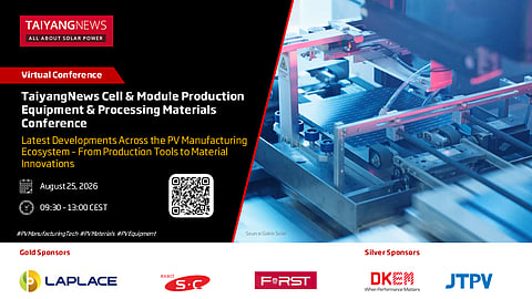
The virtual event begins in 1 hour, bringing together PV manufacturers, equipment makers, and material suppliers to discuss the latest developments across the cell and module manufacturing value chain.
The conference will cover the technology landscape from TOPCon to back-contact (BC) and tandem architectures, as well as developments in multi-cut cell layouts, zero-busbar (0BB) interconnection, metallization pastes, and encapsulation materials. The discussions will shed some light on how equipment suppliers are adapting their solutions to meet the diverse manufacturing requirements.
Stay tuned for live updates from the conference.
