

In our PERC Cell Production Equipment 2022 Report, we have looked into the key tools needed to produce a PERC solar cells – and this includes metallization devices.
Technically, a silicon wafer is a solar cell once a p-n junction is formed, but it becomes functional only after metallization is completed. The process of metallization involves depositing the metallic contacts onto both sides of the wafer and sintering them into silicon, enabling them to collect the generated charge carriers. The step also lays the platform for a series connection of cells in module making through busbars. Metallization is one of the most important processing steps in cell manufacturing that not only governs the cell's output power, but also the manufacturing costs. Developments in metallization are a collective effort from 3 different steams – metallization pastes, screen printers and screens. Screen printers have been the workhorses for the metallization process since the beginning of PV development, and screen printing is still the current state of the art. In a typical cell manufacturing line, screen printers are integrated with inter-tool transportation systems, driers, buffers, various inspection systems, firing furnace, IV testers and sorters. This completely integrated setup is often referred as the backend line. All the 3 companies part of this survey – ASYS, Maxwell and Baccini Cell Systems, a division of Applied Materials – have integrated printing lines and backend lines on offer.
The trending topics in the screen printers' section in general are high throughput, increasing production capacity per line and reducing silver paste consumption. To put it into context, the goal here is to reduce the CapEx and OpEx, and increase the throughput.
Silver consumption can be reduced by narrowing the screen opening that facilitates applying thin contacts. The screen plays a vital role here. Screens are an important and integral part of screen printers. They can be optimized to tweak important parameters of the printing process; for example, the thickness of the emulsion and mesh. Several approaches have been evaluated in this context. Polyimide (PI) based screens were popular during 2019, while knotless screens were much talked about during 2017. Stencils were considered to be effective alternatives to traditional mesh screens a couple of years earlier. However, all these approaches were short lived with the industry resorting back to standard screens. The 11 μm wire and 430 mesh screen is the mainstream, according to AMAT's CMO Giorgio Cellere.
According to the 3 suppliers, in general,the screen opening in mainstream production is between 20 and 25 μm, while the corresponding finger width ranges from 30 to 35 μm. However, paste consumption changes according to the wafer size — 112 mg for G12, 77mg for M10, and 70mg for M6, according to Maxwell's overseas business director Peter Wolf.
The latest development is, again, the ability to process larger wafers. While not apparent in the specification tables, all 3 companies confirm that they have solutions ready to process up to 230 mm formats, which are also flexible in their ability to process smaller sizes. Along with the size scale-up, the screen printer suppliers have done quite a commendable job in increasing the capacity per tool as it is evident from the fact that about 14 printing lines were required to meet a 2 GW installed production capacity cell line in 2016, while only 5 suffice now (see One Coat, Two Functions).
The screen-printers' segment was traditionally led by European suppliers such as Applied and ASYS till 2015/2016, more so the former with the highest installed base by then. Chinese companies like Maxwell have since been able to establish significant presence in the space. Maxwell has a market share of above 50%, claims Wolf. ASYS' solar sales director Matthias Drews, while not commenting on market shares, says that his company has shipped printing lines worth 6 GW in 2021. Applied has not revealed any such related information citing company policy.
Keeping the fundamentals of screen printing the same, the industry has developed a few advanced screen-printing technologies to help overcome some of the inherent bottlenecks of screen printing. The standard process has been that all the busbars and fingers on the front side are applied at once. Then came fine-line printing, which is all about reducing finger thickness. Fine-line printing brought the dual effect of reducing both shading and paste consumption – delivering on both performance and costs. The side-effect of finger disruptions followed on the heels of fine-line printing. To counter this, double printing was introduced, in which a print on print is applied. The approach not only neutralizes peaks, valleys and interruptions, if any, it also helps building the finger height, thereby safeguarding the performance even when using thinner fingers. In parallel, dual printing (different from double printing) was also implemented, which decouples the printing of busbars and the fingers. It allows for the use of separate pastes for fingers and busbars, which have different functionalities altogether. In either approach, the printing line requires 4 printers per line and a cell maker can easily switch between these printing methods without much effort.
Moving ahead, the printing table design is the most important aspect of the screen printer. The rotary table has been the state of the art for quite some time. "We invented the rotary table, which later became a worldwide standard," said AMAT's Cellere. In order to reach high speeds coupled with high print accuracy, the company had to change the architecture as the platform has a few limitations where all movements – the x, y, z and theta – are governed by the print head. In addition, the rotary table has to be rotated very precisely by 90° in order to accurately align the cell under the screen. "The entire exercise is becoming more challenging when high speeds have to be achieved and large wafer formats are used, maintaining high positioning accuracy", according to Cellere. Thus, AMAT came out with its shuttle architecture to decouple these coordinates. The X and Z axis adjustments are assigned to the shuttle, while the print head assumes the responsibility of Y and theta adjustment. The printers are provided with 2 liner shuttles to decouple the limitation of the rotary table in a way that when one cell is being printed, the cells can be loaded or unloaded on the other one. The shuttle picks up the cells from the bottom and precisely aligns them below the printing head.
AMAT's Tempo Presto LW production platform – maintaining a best in class alignment accuracy of +/- 6 μm and in a dual lane configuration – reaches a high throughput that varies according to wafer size (8,000 wafers per hour for M6, 7,400 for M10, and 7,000 for G12). According to Cellere, the tool platform supports even higher throughputs, the only limiting factor being the maximum printing speed supported by the paste. The company is also promoting a lab variant of the printer, with nearly the same specifications but offered in a single-lane configuration. As part of the complete backend line configuration, Applied has a long list of components such as loaders / unloaders, buffers, flipover, AOI, microcrack inspection systems, paste dispensing, automatic scale, cell lifters, dryers, curing furnaces, inline optical / electrical test, sorter, automatic screen cleaning, screen breakage detection, Data management system and 3D profilometer.
ASYS from Germany has 2 tool platforms available. The Airon is mainly designed to process M2 to M10 cells, and the AIRON XL for sizes M6 to G12 and above. The Airon platform also uses a new concept of moving the wafers within the machine. While sparing the details, Drews explains that the company's latest printing platform moves the wafers on pedals, while still sticking to the stationary print nest philosophy. As a result, the machines are faster, supporting a cycle time of 1 second per wafer. "We are aiming to achieve the same numbers on larger wafers as well," says Drews. At the same time, enough care is taken so that the wafers are not subjected to any additional stress. The dual-lane configuration reaches 7,200 wafers per hour for both the variants, referring to M10 wafer size, while the cycle time increases to 1.2 second with G12. ASYS' improved the degree of automation to achieve higher uptimes, mainly by reducing screen exchange time and also though line setup control via RFID technology called iSET Control. For better materials utilization, the line monitoring software suite PULSE PRO is integrated into the AIRON line.
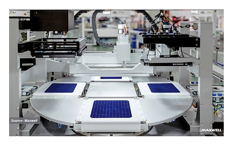
Maxwell's sole model, called MX XDLZ, still uses the rotary table design. This dual-head & dual-track solar cell metallization line provides a throughput of 7,200 wafers per hour, around 330 MW for M6 wafer and a throughput of 6,500 wafers per hour, around 500 MW for G12 wafer.
Plating
An alternative to screen printing, plating as a technology has been around for quite some time. Its entry into the mainstream, however, remains uncharted. Rena, being an expert of wet-chemical benches, has also naturally been a longtime supporter of plating solutions for metallization.
Kuehnlein provided background on plating in solar cell processing in an interview with TaiyangNews, and an update during our recent PERC conference (Watch presentation here).