

Building modules based on larger wafer formats in pursuit of the higher power is one of the most important developments in PV industry in the recent time. While the jury is still out as for what is the best size between G12 and M10, three leading vertically integrated companies are on the forefront in promoting 182 mm as the standard. The advantages of module products based on M10 wafers was also the topic on the first day of the TaiyangNews Virtual Conference on High Efficiency Solar Technologies held on Dec 1, 2020. Out of the three companies that represented the advantages of 182 mm module, JA Solar presented benefits on the manufacturing side associated with the M10 wafer format benchmarked against M6.
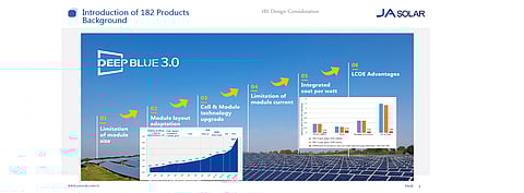
Under the title 182 mm Products Manufacturing Advantage Analysis, JA Solar's product manager Tao Wang presented the manufacturing intricacies of 182 mm wafers over 166 mm (M6) wafers along the manufacturing chain starting from growing ingots. Before going into details, he provided a list of key considerations for selecting 182 mm – module size, loading density per container, module layout adapting to current glass, equipment, cell and module technology upgrade based on current equipment and technologies, limitation of the module current for better performance, reliability and also the integrated costs per watt installation.
Production ready – crystal growth
According to Wang, the pulling rate for a silicon ingot suitable for the 182 mm wafer format is the same as that of the ingot used for G1/M6. Even the utilization rate of the ingot, meaning the proportion of ingot qualified for wafer production, is also the same as of now. Wang emphasized that there is scope for future improvements in pulling rate and ingot yield.
However, performance parity has not been achieved yet at the wafering station. While 40/38 μm thin diamond wire is used for the production of G1 wafers, M10 wafer slicing is accomplished with a slightly thicker wire of 40/45 μm. As a result, the overall wafering yield is slightly higher by 1% with 158 mm wafers, the slicing yield particularly the same for both the wafer formats. And Wang is very optimistic that M10 would equate to the level soon.
For cell processing, JA Solar identified 3 aspects as part of the risk assessment:
Ingot growth at par: M10 crystal growth rates are similar to smaller ingot sizes, according to JA Solar.
The cell reverse leakage distribution is the key for module reliability, according to JA. Data for 9 days from JA Solar's production for reverse leakage showed that more than 99% of the cells fall into a band of 0 to 0.5 A, the accepted spec in production. JA Solar has laid out a roadmap to improve cell efficiency from 22.9% to 23.1% through process optimization in all cell manufacturing steps, said Wang. The important factors in module making are high efficiency, high module power and yield, according to JA Solar, which has already attained module powers of up to 545 W corresponding to 21% efficiency. JA Solar's production data for August 22 showed that most of the production modules fell in the 540 W to 543 W power band, indicating that the majority of the production modules have 540 W and above rated power.
Not far behind: M10 cell line production yields at JA Solar are very close to the M6 process.
High power bands: JA Solar's solar module production data showed an impressive grouping of yields in high power bands.Logistics
The metric of packing density per standard 40-feet shipping container has gained importance with the increase in wafer sizes, and consequently module sizes. Wang said that the 182 mm module products feature 10 to 20% higher packing density (in metrics of kW/container), as shown in the below table. While 335 kW of M10 based modules can be shipped per container, only 285 kW can fit in the same container when supplying M6 wafer-based modules, he said.
Logistics friendly: Due to its apt width, M10 wafer based modules enable the best packing density in a typical 40-feet container, according to JA Solar.
Supply chain
With regards to production equipment for processing 182 mm wafers, JA Solar has presented a detailed list of equipment suppliers for all the manufacturing steps starting from ingot growers to module making. In terms of equipment suppliers, each production step has at least 2 to 4 qualified suppliers. JA's current mass production data shows excellent key equipment performance parameters, good product quality, high production capacity and yield rate, according to Wang.
Mature supply chain: The key materials and processing capacities needed for M10 wafer-based module production are available to enable large volume output.
JA Solar has also evaluated the status of the supply chain to support the M10 based production starting from ingot growth. The company estimates that out of the 250 GW ingot growth capacity it scouted through, 91.7% can support the 182 mm wafer format in 2021. When it comes to glass, about 50% of 220 GW glass capacity can support 182 mm based module formats in 2021. Encapsulation materials supply compatible with 182 mm module configuration accounts for 58.2% over 240 GW total capacity.
The text is an excerpt from the TaiyangNews Report High Efficiency Solar: Featuring PERC Modules with M10/182mm Cells Towards Very High Efficiency Products –A Conference Summary, which can be downloaded for free here.
A comprehensive overview on Advantages of 182mm Cell based Modules in Manufacturing was provided by Tao Wang,JASolar, during the TaiyangNews High Efficiency Solar Conference; the recording can be viewed here.