
Key takeaways:
Maxwell showcased manufacturing platforms for perovskite-HJT tandem cells, GW-scale HJT production, and copper metallization
The tandem solution scales from pilot production to commercial manufacturing and integrates key deposition technologies including CVD, PVD, and ALD
The company also presented an indium-free solution and light-induced copper plating process aimed at reducing metallization costs in HJT cell production
As perovskite-silicon tandem technology is advancing from laboratory research towards pilot and commercial-scale manufacturing, equipment suppliers are increasingly offering production solutions for this technology instead of just standalone tools. The solutions revolve around the transition toward perovskite-silicon tandem and manufacturing cost reduction.
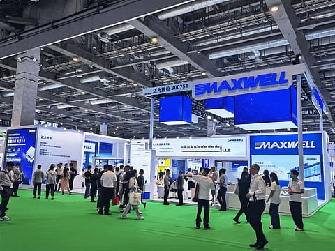
Suzhou Maxwell Technologies Co., Ltd. presented 3 manufacturing solutions targeting different stages of technology evolution and cost reduction at SNEC and Intersolar Europe 2026. First, a perovskite-HJT tandem production line; second, a GW-scale HJT production line; and finally, an indium-free copper metallization process.
The HJT-perovskite solution is designed for the 210 mm large-area format and covers the complete manufacturing sequence. The line can be configured with flexible capacity from a 20 MW pilot to a 200 MW pilot, and even a 600 MW commercial production line. According to Maxwell, the platform has demonstrated cell conversion efficiencies of over 31%. The company’s first commercial production line for HJT-perovskite technology commenced in the last week of June 2026, at a customer’s factory. The tandem production line integrates inkjet printing, chemical vapor deposition (CVD), physical vapor deposition (PVD), and atomic layer deposition (ALD).
For its GW-level HJT production line of 1.2 GW, Maxwell expanded the chambers of its core deposition tools, such as PECVD and PVD, that can support G12 and G12R wafer formats. According to the company, the theoretical output reaches 28,800 cells per hour for G12 formats and 31,200 cells per hour for G12R formats, with a production yield of 97.5%. Using 110 µm thick wafers, Maxwell claims a breakage of below 0.6%.
The third solution, which focuses on reducing metallization costs, was the copper plating process, which replaces silver-based screen printing for metallization. The solution uses a light-induced copper plating technique using a seedless approach on both sides. With this technique, the company claims to reduce metallization cost by over 50% compared to screen printing using silver. The equipment covering both patterning and metallization stages has been developed in-house and is intended for large-scale manufacturing. The company also has an indium-free transparent conductive oxide (TCO) deposition for cutting costs and finding an alternative for a scarce material such as indium.
Maxwell's showcase reflects how solar cell manufacturing equipment is evolving beyond individual process tools toward integrated production platforms. The showcase also reflects broader trends in cell manufacturing, where equipment suppliers are increasingly focusing on tandem industrialization and manufacturing cost reduction.

