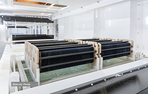

In a previous article on solar cell processing, we discussed about surface preparation steps in PERC/TOPCon cell production (see Solar Cell Surface Preparation). We now look into the texturing process. One of the key applications of wet benches in solar cell processing is texturing, which is typically combined with saw damage etching (SDE) and accomplished in an integrated setup. While SDE is a bit of an aggressive solution for removing the outer layer of silicon, texturing involves highly controlled etching. The goal of the texturing process is to realize a surface that reduces light reflection. In today's context, texturing means using an alkaline chemistry as it is suitable for monocrystalline wafers. However, acidic solutions were also in use at a time when multicrystalline was in high-volume production, and even larger than mono at some point. They are now reduced to a very small niche and face certain extinction in the not-too-distant future. This difference in chemistry also influences the mode of operation. While alkaline processing is typically done in a batch sequence, acidic solutions enabling higher etching rates support an inline mode of operation.
The 2 cost-cutting trends that were highlighted in a previous TaiyangNews market survey with regards to texturing – eliminating SDE before texturing and reducing chemical consumption – still hold good for PERC. While not exactly, TOPCon is also closely following in these footsteps. According to RENA's senior R&D manager solar & battery Damian Brunner, with TOPCon, SDE is either eliminated or very low. While the new texturing techniques and additives are still in the development phase, the latest and best results were attained with very little saw damage etch and a strongly reduced KOH consumption, says Brunner, who presented at the TaiyangNews Cell Production and Material Processing Conference 2023 (see Damian Brunner's presentation: Wet Chemical Innovations in SHJ & TOPCon Cell Processing).
As to the texturing step, first a brief update on PERC. Here, RENA is primarily promoting the classical pyramid-shaped texturing. In terms of the developments, Brunner notes that there is still some scope for optimization with regard to distribution of the classical shaped pyramids and also to reduce consumption of chemicals, especially KOH. "The ultimate goal for PERC is to bring down the reflection below 10% at 600 nm," says Brunner.
With TOPCon, RENA is working on a tweaked process using a specially designed additive that results in a different pyramid shape compared to what is found optimal for PERC. Pyramid size and distribution are the next important parameters. RENA found that close to 1 μm is where the optimal pyramid size lies at present, and the company is continuously optimizing the distribution, thus the density. The goal here is to reach reflectivity values of less than 9% at 600 nm, according to Brunner.
The texturing solution from the house of Schmid still uses the alkaline chemistry but in an inline tool configuration, which makes it somewhat special. The tool is designed to accomplish single-side processing on the front with such precision that the rear surface is completely unaffected. Schmid designed a patented pressure-less spray system called Rainbox, through which the hot chemistry is applied on the surface of the wafers. Every Rainbox in a row is replenishing the surface with fresh chemistry to realize the formation of the pyramid-textured surface. The process follows a sequence of preclean, alkaline texturing with KOH bath at elevated temperatures, followed by rinse, metal and ozone clean and final rinse, then drying. It is accomplished at 60 to 80 °C depending on the additive, while KOH and water are the other process consumables. An important characteristic of the technology is, according to Christian Buchner, Vice President of the PV business unit at Schmid, that the company's approach reduces water consumption by around 30%, etches off typically 4 to 5 μm of silicon from the surface and finally results in a reflection value of < 12% at 400 to 1,000 nm, and less than 9% at 600 nm. At the same time, the process also results in good uniformity not only within wafers, but also between wafers. The fundamental design for Schmid's tools facilitates accessibility from both sides with a catwalk separating the main process system from the chemistry cabinet and pump rooms. These production tools are based on a 10-lane configuration and are compatible with the M12 format. These wet benches use alkaline chemistry that are free from nitric acid and support a throughput of 10,000 wafers per hour with 98% uptime and are ready for the M12 wafer size with 50 μm thickness (see Christian Buchner's presentation: Innovations in Wet-Chemical Solutions).
When it comes to the listed products, the 2 tools from exateq listed here are each designed to handle SDE and texturing exclusively. Its qTex 612 texturing tool is designed for batch texturing using alkaline media. The tool accepts wafers up to a size of G12. Each process basket accommodates 104 of such wafers, and the loading and unloading of the substrates can be done both automatically as well as manually. The tool consists of 4 baths for active processing and 7 for rinsing and cleaning, processing up to 12,000 wafers per hour with a rated mechanical yield loss of less than 0.1% and a 95% uptime.
qEtch 612 SDE, the company's SDE tool, is also built on the same configuration. Except for the application, it differs very little from its texturing counterpart. This system also uses KOH as the process chemical, and hydrogen peroxide, HF and HCL as the cleaning agents. It has 4 chemical baths and 5 baths for cleaning and rinsing. The maximum throughput of the system is 12,000 wafers per hour. The only notable difference according to the listed specifications is its length of 20 m, while the texturing tool measures 26.3 m. Out of the 2 products listed from RENA, BatchTex 3 N600 is the latest, which handles a batch size of 600 to 720 wafers at a time, achieving a throughput of up to 15,000 wafers per hour for M6, and a slightly lower 12,500 for M10/M12. The earliergeneration BatchTex 2 N400 XL Combi is still part of the company's product portfolio that handles a batch size of 400 wafers with 100 wafers loaded in each of the 4 baskets. This tool reaches a maximum throughput of 8,000 and 7,000 wafers with M6 and M10/G12 wafer formats, respectively. We have data for 3 models from Schmid; apart from the above discussed alkaline texturing tools, Schmid has also listed its previous generation tools based on HF / HNO3 chemistry.
S.C New Energy, the leading tool vendor from China, has provided data for 2 products – SCCSZ8000E- 16F and SC-CSZ14400F-17G. The company chose to leave several fields blank in the specification tables, and according to the available information, both the tools are for SDE and texturing, and both use alkaline chemistry. The key difference: SC-CSZ8000E-16F is designed to handle a batch of 400 wafers, while the SC-CSZ14400F-17G is capable of handling 600 to 720 wafers at an hourly throughput of 15,120 M10 wafers. The capacity drops to 9,600 wafers with the G12 size.
This section of the market survey also lists 2 products that are somewhat special, in that they are actually not wet-chemical tools at all. The 2 tools from Nines Photovoltaics ("Nines PV") are based on atmospheric dry etching. As an alternative to the wet-chemical solutions, be it to realize SDE or texturing, Nines PV has developed a proprietary process called ADE, which stands for Atmospheric Dry Etching. The company has been developing this process since 2010. What makes this technology unique is that it accomplishes dry texturing at atmospheric pressure using fluorine (F2) as the etching gas. This eliminates the need for vacuum and plasma – both key ingredients and cost drivers in typical dry etching technologies. Also, the technology has no special adverse impact on the environment. The thought of fluorine as an etching gas itself rings alarm bells about greenhouse gases. However, as detailed in our previous survey, the molecular fluorine used by Nines PV scores a zero against the commonly used SF6 that has high global warming potential, as emphasized by CTO Laurent Clochard.
The technology fits best for etching, especially in etching the silicon wraparound in TOPCon, but not limited to. Nines PV has tweaked this technology to realize texturing, and the benefits here are that: a) it is a single-sided process that alleviates the need for rear polishing, and b) it removes less silicon than an alkaline process which helps achieve lower reflectivity facilitated by the sub-micron scale texture, according to the company. Nines PV is promoting 2 variants – ADE3000-SS NANO-TEX and ADE6000- SS NANO-TEX. Both the tools process wafers up to the G12 size. However, the latter processes M6 to G12 wafers in 4 lanes with a rated throughput of 6,000 wafers per hour. The number of lanes is exactly half in ADE-3000, so is the throughput. The company is also willing to supply an R&D-scale system with a single lane of transport.
The article is an excerpt from the TaiyangNews Market Survey on Solar Cell Production Equipment 2023, which also includes detailed product specs and can be downloaded for free here.
