
Key takeaways:
Existing PERC lines can be adapted to manufacture p-type IBC cells using modified process steps
Metallization optimization shows trade-offs between contact resistance and recombination losses
Reducing polysilicon thickness lowers carrier absorption but also impacts Voc, requiring further optimization
Almost all the PERC players of the early 2020s have now become major TOPCon manufacturers. With several new players entering the market, TOPCon has now become the mainstream cell technology. Most of these TOPCon capacities were newly built rather than being upgrades of existing PERC lines.
With back contact (BC) seen as the successor to TOPCon, researchers at ISC Konstanz and Fraunhofer ISE are working to convert these PERC lines into p-type-based IBC (pIBC) lines. The advantages of pIBC include its reduced reliance on silver and a low thermal budget during diffusion as compared to TOPCon.
The idea is to bring together the mature metallization process of the PERC’s p-type base and the existing TOPCon metallization process of the n-type poly-Si side. As part of this study, M2-sized Ga-doped CZ wafers were processed to make IBC cells. The front side is textured to form random pyramids, while the rear side is polished for making n- and p-type interdigitated contacts. First, a thin SiOx layer is thermally grown, followed by phosphorus-doped a-Si deposition using PECVD. After annealing in an O₂ atmosphere, n-polySi crystallizes. Using laser ablation, interdigitated patterns are created to form the base layer (p-type) for Al-paste metallization, and the n-polySi region for Ag-paste metallization. The study involves commercialization of this process by optimizing metallization and n-polySi thickness.
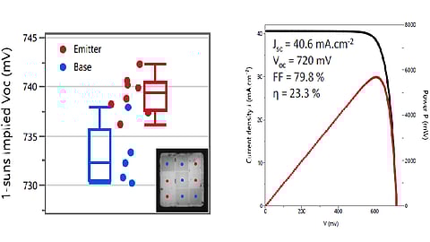
The bottlenecks for using aluminum paste are metal contact recombination and contact resistance in the base region. Experiments with varying amounts of silicon in Al-paste were conducted. The contact resistance (mΩ·cm²) was calculated using the transfer length method (TLM), while the implied Voc (iVoc) loss for varied Si content in Al-pastes was obtained using photoluminescence (PL) image processing. The team observed a trend of increasing contact resistance with increasing silicon content in Al-pastes and lower firing temperatures. It also observed that the iVoc loss after metallization increased with increasing silicon content.
The polysilicon layer contributes to free carrier absorption. Therefore, in this study, the thickness of the n-polySi region was varied to further optimize the process, analyzing the effects of these changes. Researchers observed a gain in short-circuit current (Jsc) with decreasing thickness of n-polySi, which directly reflects the reduction in carrier absorption. However, there was a reduction in Voc. The study, titled Development of a p-type Silicon Interdigitated Back Contact Solar Cell With Passivated Contacts, concludes that further research is required to understand this behavior.
pIBC cells prepared using the above optimization techniques were presented with a champion cell recording an efficiency of 23.3% with a Voc of 720 mV and a fill factor (FF) of 79.8%.

