

As perovskite-silicon tandem solar cells move toward industrialization, reliable characterization becomes essential due to the added complexity of monolithic 2-terminal architecture
Conventional silicon measurement protocols face limitations in tandem devices, particularly in I-V spectral matching, perovskite metastability caused by ion migration, and lateral inhomogeneities across large-area wafers
The study proposes industry-compatible solutions, including spectrally tunable LED-based I-V testing, controlled preconditioning protocols, and advanced luminescence imaging for inline defect detection
As perovskite-silicon (Pero/Si) tandem solar cells advance toward industrial manufacturing, characterization and quality control are emerging as critical bottlenecks. While tandem architecture promises higher performance than conventional single-junction devices, its monolithic structure introduces new measurement complexities that cannot be addressed using established silicon testing protocols.
A recent study published in Solar RRL examines measurement bottlenecks specific to monolithically stacked tandem solar cells. The work was led by Fraunhofer ISE in collaboration with the University of Freiburg, ODTÜ-GÜNAM, and industrial metrology partners including ISRA VISION, Wavelabs, and halm elektronik. The authors identify 3 central challenges: accurate I-V characterization, perovskite metastability, and lateral inhomogeneities in large-area devices.
I-V Analysis in Monolithic Tandems
Monolithic tandem cells contain 2 series-connected subcells with different spectral responses. This differs from single-junction silicon cells. The perovskite top cell and silicon bottom cell share only 2 electrical terminals, which prevents independent probing using standard I-V methods. Accurate power measurement, therefore, requires precise spectral matching between the solar simulator and the current-limiting subcell.
Conventional solar simulators optimized for silicon cannot independently adjust spectral components. Multi-channel LED solar simulators with programmable spectral tuning are used to address this limitation. By adjusting spectral composition, subcell currents can be balanced, reducing spectral mismatch errors within IEC compliance limits.
The researchers further introduce a rapid quasi-external quantum efficiency (qEQE) approach that enables approximate subcell current extraction within milliseconds, making it compatible with inline industrial testing. Without spectral adaptation, the authors show that standard A+ simulator spectra can lead to current mismatches of several percent, potentially masking real performance losses or inflating reported efficiency values.
In this collaboration, Wavelabs contributed LED-based solar simulation platforms enabling spectral control, while halm elektronik supported the integration of tandem-compatible I-V concepts into industrial testing environments.
Perovskite Metastability
A second challenge arises from the inherent metastability of perovskite materials. Ion migration under illumination and electrical bias can induce temporary changes in device behavior, leading to hysteresis in I-V curves and time-dependent variations in fill factor and maximum power point.
The study shows that measurement outcomes depend strongly on scan speed and preconditioning procedures. Very fast scans can artificially inflate measured power due to transient capacitive effects, and insufficient light preconditioning leads to unstable results. Experimental data indicate that even short illumination stabilization periods are necessary to obtain reproducible measurements.
These findings suggest that conventional silicon testing protocols cannot simply be transferred to tandem architectures. Instead, standardized stabilization routines and controlled measurement sequences will be required for reliable industrial implementation.
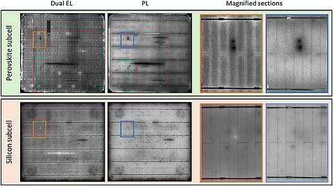
Lateral Inhomogeneities in Large-Area Tandems
With tandem scaling to larger wafer formats, spatial variations in perovskite layer thickness, crystallization quality, and interface formation become increasingly critical. Such lateral inhomogeneities can introduce localized current mismatches that are not captured by global I-V measurements.
To address this, advanced luminescence imaging concepts for inline quality control are presented. These include dual-camera electroluminescence (EL) systems with junction-specific filtering, line-scan photoluminescence (PL) setups, and simplified RGB-based imaging capable of separating perovskite and silicon subcell signals.
Industrial imaging tools from ISRA VISION were used to validate inline-compatible luminescence inspection concepts for detecting thickness variations, interlayer defects, and localized performance losses.
The research was published in Solar RRL under the title “Industrial Production of Perovskite–Silicon Tandem Solar Cells: The Characterization Challenge.”
