

Crystal-growth and wafering platforms must support the different quality requirements of TOPCon, HJT, BC and future tandem cells
Kulkarni expects productivity to increase by more than 100% and costs to decline by around 30% to 40% on existing equipment platforms
RSOLEC plans to localize graphite, quartz and other crystal-growth consumables in India
Advances at the solar cell level are placing new demands on upstream processes such as crystal-growth and wafering. These platforms are expected to support TOPCon, heterojunction (HJT), back-contact (BC), and future perovskite-silicon tandem cells. Manufacturers must also accommodate larger and thinner wafers while reducing kerf.
Speaking at the TaiyangNews Cell & Module Production Equipment & Processing Materials Conference 2026, Milind S. Kulkarni, Chairman and CEO of RSOLEC, said these changes will largely need to be achieved on existing Czochralski crystal-growth and diamond-wire-saw platforms. Kulkarni noted that the industry has moved from multicrystalline and p-type technologies to n-type monocrystalline silicon and TOPCon over the past 15 years. Wafer thickness has also fallen from around 200 µm to approximately 130 µm for TOPCon. HJT manufacturers can use even thinner wafers of around 100 µm.
He expects productivity on existing crystal-growth and wafering equipment to more than double over the next three to five years, supported by improvements in equipment design, processes, and control systems. However, higher throughput must not affect wafer properties. “Quality is not negotiable,” Kulkarni said, adding that manufacturers must control crystal diameter, dislocations, oxygen concentration, resistivity, impurities, and microdefects while accommodating different wafer formats and cell requirements.
Controlling Oxygen & Resistivity
Oxygen requirements have become stricter with the adoption of high-temperature cell processes such as TOPCon. Kulkarni said acceptable oxygen concentrations have declined from approximately 18 PPMA around 15 years ago to about 9 PPMA for some current applications. HJT manufacturers can accept higher concentrations of around 14 PPMA.
Lowering the oxygen concentration alone may not prevent oxygen precipitates. Manufacturers must also control vacancies in the silicon crystal, as their interaction with oxygen can affect minority-carrier lifetime and contribute to ring defects in TOPCon cells. Kulkarni also identified resistivity uniformity as an important challenge. Conventional batch Czochralski growth produces resistivity variations as the melt solidifies. He presented continuous Czochralski (CCZ) growth, already used for semiconductor applications, as a potential route to a more uniform resistivity profile across the ingot.
The process could provide tighter resistivity control, but oxygen incorporation would also have to be managed through crystal-puller design and process conditions. Kulkarni said CCZ growth is unlikely to enter mainstream solar production immediately but could gain market share over time.
Simulation & Metrology
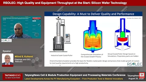
Kulkarni presented simulation and experimental results showing that process changes within the same crystal-puller design can alter temperature distribution, melt flow, the crystal-melt interface, and oxygen concentration. This flexibility could allow manufacturers to meet various customer specifications without replacing the complete puller.
At the wafering stage, thinner wafers, smaller wire diameters, lower kerf, and faster cutting can affect wafer geometry, surface characteristics, and subsurface damage. Diamond wires and slicing conditions can also influence how wafers respond to subsequent texturing and cell processing. Therefore, he emphasized the need for in-house simulation, equipment design, and metrology capabilities. Simulation results must be compared with experimental measurements before introducing process changes at manufacturing scale.
According to Kulkarni, equipment suppliers cannot provide long-term differentiation because they generally offer similar equipment to multiple customers. Tier 1 manufacturers instead differentiate themselves through proprietary hot-zone designs, control algorithms, and production processes.
Localizing Consumables
Interacting with the moderator after his presentation, Kulkarni highlighted the cost and performance implications of crystal-growth consumables. Excluding polysilicon, graphite, quartz, and other consumables account for around 10% to 15% of crystal-growth costs. These components also influence equipment productivity and crystal quality.
RSOLEC plans to work with local vendors to develop these consumables in India, while using its simulation and design capabilities to support this localization. Kulkarni emphasized that the company focuses on consumables rather than complete crystal pullers, which have much longer operating lives. He added that consumables may require replacement approximately every 8 months, while Tier 1 manufacturers typically redesign them every 18 to 24 months.
Kulkarni believes India has the manufacturing capabilities to establish this supply chain, provided companies develop the necessary design and simulation expertise.
The full presentation is available on the TaiyangNews YouTube channel.
