

S.C New Energy discussed key manufacturing challenges associated with perovskite-silicon tandem solar cells, including substrate cleanliness, film formation, and edge-effect control
It highlighted cleaning approaches for TOPCon and HJT bottom cells, including functional-water technology based on micro-nano bubbles to reduce particle contamination and modify oxide surfaces
The company also presented its tandem manufacturing infrastructure, including inkjet-printing systems, vacuum coating technologies, and a perovskite pilot production line designed for future GW-scale industrialization
Perovskite-silicon tandem solar cells are increasingly transitioning from laboratory-scale development toward pilot-scale manufacturing, bringing greater attention to scalable processing and equipment integration. Beyond achieving high conversion efficiencies, tandem production also requires precise substrate cleaning, uniform thin-film deposition, and stable large-area processing compatible with industrial throughput.
At the recent TaiyangNews Conference on Next-Generation PV Technologies, Yongqiang Zhang, Technical Engineer at S.C New Energy, discussed the company’s approach to mass-production technologies for perovskite-silicon tandem solar cells. His presentation focused on cleaning technologies, vacuum coating processes, inkjet printing, and pilot-line development for tandem manufacturing.
Several bottlenecks remain in tandem mass production, including maintaining substrate cleanliness throughout the fabrication process, achieving high-quality film formation on textured surfaces, and controlling edge effects during deposition.
Zhang discussed tandem device structures that combine perovskite top cells with TOPCon or HJT silicon bottom cells. He presented a process flow in which physical vapor deposition (PVD) is used to deposit intermediate layers such as ITO and metal oxides, while self-assembled monolayer (SAM) and perovskite layers are processed through inkjet printing. Additional functional layers, including electron transport layer (ETL) materials, can then be deposited by evaporation, followed by buffer-layer deposition via reactive plasma deposition (RPD) or atomic layer deposition (ALD) and final transparent conductive oxide (TCO) formation using IZO.
Substrate cleanliness remains one of the key challenges in tandem fabrication. TOPCon and HJT surfaces typically contain oxides, dust, and particles that can significantly affect tandem device performance if not properly removed. Therefore, S.C recommended different cleaning approaches for each bottom-cell technology: a single-sided, precise chemical-control chain-cleaning process for TOPCon cells and double-sided batch cleaning for HJT cells.
The cleaning sequence includes ultrasonic cleaning, functional water treatment, pure water cleaning, slow lifting, and vacuum drying modules. One of the technologies highlighted during the session was functional water, also referred to as micro-nano bubble water < 100 μm. Negatively charged bubbles can adsorb positively charged contaminants and particles, while bubble rupture generates localized micro-jets that help clean substrate surfaces. Bubble collapse can also generate hydroxyl radicals and reduce liquid surface tension.
Experimental results showed lower particle counts on substrates cleaned with functional water than on those cleaned with conventional methods. The treatment was also linked to oxide-surface modification through the formation of additional OH groups, which are considered beneficial for SAM-layer coating and substrate bonding.
Vacuum coating technologies formed another major focus area for tandem manufacturing. Zhang outlined multiple deposition platforms, including tube-type, plate-type, and roll-to-roll equipment for perovskite, silicon, TOPCon, HJT, and tandem solar cell fabrication. He also highlighted PVD deposition for layers such as NiOx, AlOx, ITO, and IZO for its high film density, strong adhesion, and large-area uniform coating capability.
Also part of his presentation was a discussion of evaporation processes for depositing ETL materials such as C60 and additional functional layers. These processes can achieve film-uniformity variation below 3% while operating at substrate temperatures below 80°C. The company also uses RPD and ALD technologies to deposit buffer layers such as IWO and tin oxide, while Plasma-enhanced chemical vapor deposition (PECVD) and hot-wire CVD are used for anti-reflection layer formation. Spatial and temporal ALD approaches were also discussed for tandem processing.
Inkjet printing was another major focus area, particularly for large-area tandem processing. The company demonstrated inkjet processing on 210 mm half-cell tandem substrates while controlling droplet volume between 1 pL and 10 pL. The systems also support controllable perovskite-film thicknesses ranging from 300 nm to 800 nm and compatibility with multiple precursor solvents, including DMF, DMSO, GBL, and chlorobenzene.
The inkjet-printing process achieved film-thickness variation below 5%, with some cases approaching 3%. Edge-effect control below 10 μm during inkjet processing was also highlighted as an important factor for improving deposition precision in tandem fabrication. The process also incorporates nozzle anti-clogging and precise droplet-control approaches for stable large-area deposition.
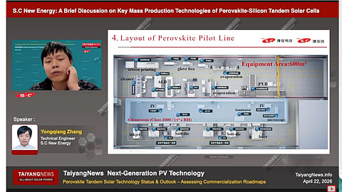
S.C New Energy also operates a perovskite pilot production line in Changzhou, which is equipped with more than 20 sets of tandem manufacturing equipment, including slot-die coating, inkjet printing, evaporation, laser systems, PVD, ALD, and cleaning technologies. Only the central processing zone is maintained under Class 1000 cleanroom conditions with humidity near 10%, while outer zones remain outside the controlled environment to reduce operating costs.
Zhang added that several key industrialization challenges related to perovskite stability, efficiency, and equipment localization are gradually being addressed. He said large-scale mass production of perovskite solar cells could become feasible around 2030 following further production and field verification stages.
The full presentation titled “A Brief Discussion on Key Mass Production Technologies of Perovskite-Silicon Tandem Solar Cells” is available on the TaiyangNews YouTube channel here.
