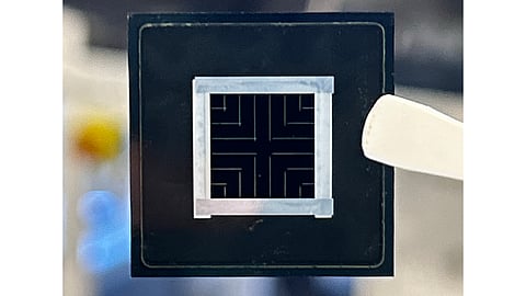


University of Freiburg and Fraunhofer ISE researchers developed a perovskite-HJT tandem cell with a solvent-free top cell
The perovskite absorber was deposited through sequential thermal evaporation
Textured silicon enabled more effective conversion of the deposited materials into perovskite than planar silicon
Researchers from the University of Freiburg and the Fraunhofer Institute for Solar Energy Systems ISE have developed a 2-terminal (2T) perovskite-silicon tandem solar cell combining a solvent-free perovskite top cell with a silicon heterojunction (HJT) bottom cell. According to the researchers, the device achieved an efficiency of 27.3%.
Perovskite layers are commonly deposited from liquid solutions. However, the solvents used in these processes can raise toxicity concerns and make it harder to achieve uniform films compatible with the other cell layers.
The Freiburg team avoided solvents by producing the wide-bandgap perovskite top cell using vacuum-based deposition processes, including thermal evaporation, atomic layer deposition, and sputtering. The perovskite absorber was deposited through sequential thermal evaporation. The starting materials were applied one after another and then heated to form the final perovskite layer.
The work was carried out by the Optoelectronic Thin-Film Materials Junior Research Group at the University of Freiburg’s Department of Sustainable Systems Engineering (INATECH), together with Fraunhofer ISE. The research team, led by Mohamed A. A. Mahmoud and Dr. Juliane Borchert, used in situ X-ray diffraction to monitor perovskite formation during evaporation and subsequent annealing. They also compared the process on planar and microtextured silicon substrates.
The study showed that the silicon surface structure affected perovskite layer formation. On planar silicon, the deposited lead-halide layers formed a comparatively compact structure. On textured silicon, the layers were more porous, allowing the materials to mix and react more effectively.
As a result, a greater proportion of the deposited materials was converted into perovskite on textured silicon. The researchers detected a residual unreacted lead iodide layer on the planar substrate, while no distinct lead iodide layer was found on the textured substrate after processing.
The team also observed bromide and iodide redistribution during annealing. The temperature and atmosphere used for this step affected perovskite formation and device performance. Higher processing temperatures improved performance but also affected the stability of some hole-transport materials. According to the researchers, this must be considered when selecting materials for the top cell.
For the tandem device, the team deposited the hole-transport, perovskite, passivation, and electron-transport layers without using solvents. The evaporated passivation layer improved the electronic properties of the perovskite surface and may also have penetrated deeper into the absorber.
After 6,800 hours of storage in nitrogen and darkness, the cell retained 97.06% of its initial efficiency. This represents shelf-storage stability rather than performance under illumination or outdoor operating conditions.
Borchert said that moving perovskite-silicon tandem cells from laboratory development to industrial manufacturing requires the right combination of deposition methods for reliable, large-scale, and high-throughput production.
The researchers collaborated with Martin Luther University Halle-Wittenberg in Germany, Universidad Pablo de Olavide in Spain, King Abdullah University of Science and Technology in Saudi Arabia, and the ODTÜ-GÜNAM research center in Türkiye.
The study, titled Impact of silicon substrate topography on sequentially evaporated perovskite film growth, was published in Joule.
