

HJT technology generally carries an image of a premium solar cell technology that is expensive. It is true that the manufacturing costs are higher than for PERC. A contributor to higher cost is the wafer type itself. Unlike the main stream technologies such as PERC, which uses p-type wafer as base, HJT cells are generally produced using n-type wafers. In s previous article, we have already described key cost drivers, including high grade polysilicon, low level of REZ content, no market for low grade wafers, among others (see Breakdown of Higher Costs n-type Wafers).
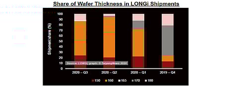
That means there is plenty of cost reduction potential. One means to cut cost at the wafer level is thinning down the silicon slices themselves, a rather direct approach. Reducing the wafer thickness by 10 µm reduces the wafer costs by $0.01. And the thickness reduction is more aggressive with n-type technologies compared to p-type. According to Yichun (YC) Wang, director of application engineering and key customer service at LONGi Silicon, the n-type market is shifting from 170 µm to 160 µm and some are already evaluating 150 µm, as shown in the graph. The data here, though, can serve just as an example, as the absolute numbers may not have significance given the share of n-type in global wafer supply where even a small change can show a huge variance.
The TaiyangNews Report on Heterojunction Solar was launched during our High Efficiency Solar Technologies Conference 2020 in Dec. 2020. For detailed information regarding wafer thickness and costs, please download and read the report for free here.