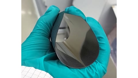


Researchers fabricated an ultra-thin 80 µm silicon solar cell using a biPoly architecture with selective front n-type TOPCon and full-area rear p-type TOPCon passivated contacts
The cell achieved a power conversion efficiency of 19.7% and an efficiency-to-thickness ratio of 0.25% per µm
The ultra-thin cells demonstrated mechanical flexibility, highlighting their potential for lightweight applications
The rising cost of materials has pushed manufacturers to adopt increasingly thinner wafers. In addition to lowering material consumption, reducing silicon wafer thickness also makes solar cells lighter – an attractive proposition for applications such as building-integrated photovoltaics (BIPV), portable power systems and wearable electronics. However, thinner wafers are more fragile. They are also more susceptible to recombination losses, making it difficult to maintain high performance levels.
Researchers from the National University of Singapore (NUS), the Solar Energy Research Institute of Singapore (SERIS), and AGH University of Krakow explored the extent to which silicon wafer thickness can be reduced while maintaining good device performance.
The study reports an 80 µm biPoly TOPCon solar cell achieving a power conversion efficiency of 19.7%. For comparison, mainstream TOPCon production today typically relies on wafers around 120-160 µm thick. This cell employs passivated polysilicon contacts on both sides of the wafer, commonly known as a biPoly or double-sided TOPCon structure.
While these contacts provide excellent surface passivation, the front-side polysilicon can absorb a portion of the incident light, reducing the amount reaching the silicon wafer. To address this, the researchers adopted a selective n-type TOPCon design. The n+ polysilicon layer was retained only beneath the metal fingers rather than across the entire front surface. The rear side continued to use a full-area p-type TOPCon contact. By limiting front-side polysilicon coverage, the design reduces parasitic absorption while maintaining the passivation benefits of TOPCon contacts.
To study the impact of wafer thinning, the researchers reduced the thickness of industrial n-type silicon wafers from 180 µm to 80 µm using a saw damage etching process. Removing saw damage initially improved carrier lifetime. However, performance began to decline as the wafers became thinner. Recombination losses became increasingly significant at lower thicknesses. This is addressed by incorporating an ultra-thin tunnel oxide, polysilicon-passivated contacts, and a silicon nitride (SiNx) capping layer.
The SiNx capping layer significantly improved surface passivation. It increased carrier lifetime and implied voltage while reducing surface recombination losses, as summarized in the table above. The paper attributes these improvements to enhanced passivation and hydrogenation at the silicon/poly-Si interfaces.
The study also compared ex-situ and in-situ doping approaches for the polysilicon layers. In the in-situ process, dopant gases were introduced during LPCVD deposition. This avoided vacuum breaks between tunnel oxide formation and polysilicon growth. Compared with ex-situ doping, this approach reduced surface recombination current density by approximately 36%.
For device fabrication, the researchers combined front-side texturing, selective polysilicon patterning, laser contact opening, and screen-printed metallization. This process was applied to M2-sized wafers thinned to 80 µm. Only 6 cells survived the complete fabrication sequence. This highlights one of the practical challenges associated with ultra-thin silicon wafers.
Following metallization, the best-performing cell achieved a power conversion efficiency of 19.7%. The highest fill factor exceeded 83%. When normalized to wafer thickness, the resulting efficiency-to-thickness ratio reached 0.25% per µm. The study notes that this compares favorably with previously reported TOPCon devices fabricated on thicker wafers.
The findings were reported in the paper titled Ultra-Thin Bipoly Solar Cells With Front Selective n-Type TOPCon and Rear Blanket p-Type TOPCon Layers.
