

The technical developments in the wafering part of the PV value chain cannot be labeled with one common trend. This is the first impression when comparing the technology progress forecasted for wafering in the 2014 edition with the 6th edition from 2015 of the International Technology Roadmap for Photovoltaic (ITRPV), which was released in spring 2015 and updated in the summer. The developments in areas such as the share of diamond wire technology for multicrystalline silicon wafers and the emergence of alternate wafering techniques are at par to last year's predictions. But the progress in reducing kerf loss and wafer thickness as well as the spread of full square wafers are expected to be further delayed. The improvements in throughput for slurry based sawing technology is an aspect, which surpassed previous expectations. However, the 2015 edition has skipped or not provided adequate information for as many as 8 topics, which were part of the previous version. Still, the 2015 roadmap covers the most important areas of wafer making.
Diamond cut for multi will dominate
Diamond wire based sawing is the hottest topic in wafering. While slurry based sawing continues to be state of the art, employing this fixed abrasive method for producing silicon slices has been growing due to its numerous advantages. Diamond wire based sawing is not only twice as fast as the standard slurry method, it also has a higher potential to reduce manufacturing costs, especially on account of its better ability to reduce kerf loss and no need to buy and recycle the slurry. Moreover, the wafers produced using diamond wire have lower subsurface damages, which improves the quality of the final product
Diamond wire based sawing is maturing and is quickly making its inroads into monocrystalline wafering. Mono-wafer makers adding new machines usually buy diamond wire saws. Adapting the technology for multicrystalline material has already started as well, according to the new ITRPV edition. In fact, its view on diamond wire sawing for multicrystalline silicon has not changed. The 2015 roadmap also estimates that diamond wire based sawing of multicrystalline would have a market share of about 5% in 2015 and would eventually dominate the slurry process by gaining more than half of the market in the next 10 years. However, the 2015 study has not provided any status update on the technology's share in monocrystalline sawing. If the previous year's values hold good, it should have gained a considerable presence of about 25% in the monocrystalline segment – but this is unlikely as capex spending for new wafer equipment is just starting.
Slurry would do better
The 2015 roadmap expects considerable improvements in throughput. The throughput increases for both slurry and diamond wire based sawing tools are supposed to have the same rate until 2022 – that is 120% over the 2014 level. However, in the following 3 years until 2025 no throughput improvement is expected in slurry technology, while diamond wire process will reach 130% wafers per hour. Compared to 2014, ITRPV is positively looking at the developments in the slurry segment, while the projection has remained nearly unchanged for diamond wire. The previous version depicted a meager throughput enhancement in slurry sawing tools – reaching 105% in 2018 and close to 115% in 2024. Unfortunately, the 2015 study has not provided any reason for its revised positive outlook about the slurry process.
However, as noted in the 5th edition, structured wire sawing can bring significant throughput advancements. This method to cut wafers is also based on the "loose abrasive" principle, so it belongs to the slurry category. But instead of a typical straight wire, structured wire sawing employs a crimped wire, which – due to its shape – enhances slurry supply to the cutting area, enabling around 20 to 30% higher cutting speeds.
Yield improvement in focus
More than throughput, the 2015 roadmap emphasizes improvements in yield, mainly through reducing kerf loss, which will have a more pronounced effect on the productivity than the throughput improvement at the tool level. The logic is simple – the lower the kerf, the higher is the number of wafers obtained per brick. Using slurry based sawing, around 150 µ m material is lost and for diamond wire you loose around 130 µm – both of which are expected to decrease by another 25 µm over the next 10 years. This current projection indicates that ITRPV was overoptimistic on the developments contributing to kerf reduction in the past. The 2014 roadmap expected wafer makers to attain a kerf loss of 140 µm for slurry and 130 µm for diamond wire already in 2014 and then gradually further decrease by 30 µm and 40 µm by 2021, respectively – and remain unchanged from then on.
Few more subjects not covered
The diameter of sawing wire is a key component in reducing kerf. While the 2015 roadmap emphasizes that wire diameters will be reduced considerably in the coming years, details are missing on the extent. The
particulars given in the 2014 roadmap may not be valid in absolute terms, as the prognosis for kerf reduction is considerably revised. However, since the relation between kerf loss and wire diameter is the same, the previous data serves as reference for approximation that the wire diameter reduction in the next 10 years is about 20 µm for both standard and diamond wire. While the latter would slim down from 100 to 80 µm, the slurry wire thickness will be reduced from the current level of 120 to 100 µm. The silicon carbide and diamond grit size also contribute to kerf reduction, but are not discussed in the 2015 roadmap. The previous study also anticipated a reduction in the price of the process consumables by 5 to 10% per year and especially the need to lower the price of diamond wire to 25% in 8 years. The 2015 study has not provided any updates on these aspects. But, on the other hand, it does underscore that the PV industry increasingly focuses on recycling, especially silicon and diamond wire, both of which have high potential for cost savings. The well established recycling of silicon carbide is expected to stay at 80%.
Like the year before, the 2015 roadmap is not optimistic about the prospects of alternative wafering approaches, such as kerfless technologies, which are not even expected to gain a 5% share by 2025. That's mainly because the established sawing technologies are evolving so strong that they are creating a high level entry barrier for new technologies.
No, wafers are not on a diet
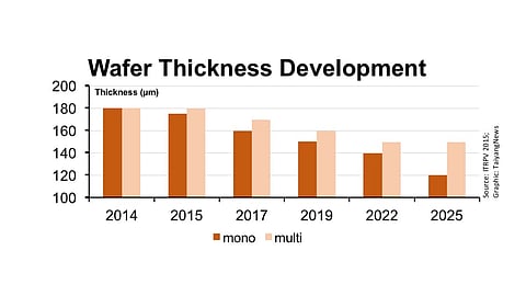
As wafers still contribute the highest share to the cell price, though down from last year's level of 57% to about 51% now, ITRPV has been a strong advocate of reducing wafer thickness. But its previous predictions, including those from last year, have not come true. The falling silicon prices as well as the higher risk of breakage associated with thin wafers is interrupting this transition. The preferred wafer thickness in today's mass production is still at 180 µm, that's nearly unchanged from last year's level. The 2015 study expects that multicrystalline wafer thickness would reduce to 170 µm only by 2017 and then to 150 µm in 2022. Monocrystalline wafer thickness is expected to move differently. While the thickness was the same as for multi last year, it will thin down by 5 µm to about 175 µm this year and decrease consistently to 140 µm by 2022. In the following 3 years, a steep dip is expected, which will result in 120 µm thickness. Adding to that, the wafer thickness reduction drive in monocrystalline would be governed by the limit of cell thickness specified by future module technologies, which are expected to create a demand for thin wafers – 150, 125 and 100 µm in 2017, 2019 and 2022, respectively. The 2014 roadmap had predicted the limit of cell thickness in alternate module technologies would take a sharp decline much earlier, between 2016 and 2018, and the magnitude was also high – from 125 µm to 50 µm, respectively, and would go below 25 µm between 2021 and 2024.
Full square wafers have to wait
Coming to the wafer format, the 2015 roadmap anticipates pseudo square wafers would remain the standard and full square wafers slowly penetrate into the market – from a 2% share today to about 20% in the next 10 years. The previous edition forecasted a more than 30% share for full square wafers already in 2018. It also gave a spec for a 10% Total Thickness Variation (TTV) of the wafer and forecasted that costs as well as the price of mono wafers would be 20 to 30 higher than from casted origin. A price gap was also expected to continue between p-type and n-type mono crystalline wafers, at least until 2018. The 2015 study has skipped these two topics as well.
Work in progress
Ignoring the aspects that have not been reported on, the wafering segment has certainly made progress. Diamond wire technology, after meeting the expectations in monocrystalline sawing, is now about to making its first steps into multicrystalline wafering. The technology is expected to dominate the slurry process in 10 years. However, slurry based sawing – also with the help of structured wire – has been able to attain higher throughputs beyond expectations. The progress on reducing wafer thickness and kerf loss is not up to the level as expected. And especially regarding the reduction of the wafer thickness, projections still seem optimistic, especially when looking back. Overall, although developments in wafering are missing a common trend, you can see progress. Or better call it "work in progress".