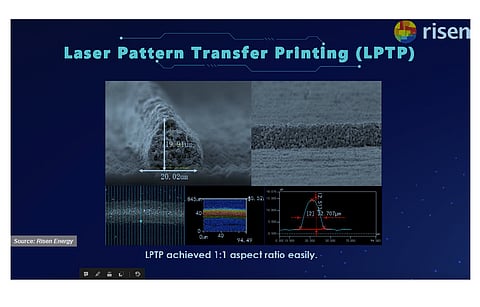


In our recent articles on HJT cell processing we also mentioned several approaches explored in metallization of HJT (see Developments In Metallization For HJT). We now look further into alternate methods to improve the metallization process. Laser Pattern Transfer Printing is another method to improve metallization of HJT, and Risen is working on this technology. This approach is an alternative to screen printing, but it still uses a paste system. Here, the grooves are filled with paste which is then transferred on to the cell via laser. The benefit of this approach is that it can attain a very good aspect ratio of 1 and the method is non-contact, thus supporting very thin wafer processing.
Copper plating has not only been a long-term candidate for metallization of HJT cells, it has also been commercially available for a long time. As discussed in the previous editions of our HJT report, it was mainly Dutch company Meco that was promoting a plating-based solution for metallization of HJT cells. Then, GS-Solar, a Chinese HJT producer that turned into an equipment supplier, also promoted plating aggressively until a couple of years ago, but later shifted to screen printing. However, the technology is now attracting new followers, and the leading equipment supplier is Maxwell.
The company is currently working on a seed and plate approach in which the copper seed layer is applied via sputtering, followed by masking the non-metallic area with photosensitive material and opening the contacts by exposure. Then, the electroplating of copper is accomplished simultaneously on the front and rear sides, followed by a photoresist strip and tin plating. The formation of metallic contacts is finished with annealing.
Maxwell is cooperating with several partners to improve the process and introduce plating in mass production industrial environment, according to Peter Wolf, Maxwell's VP Overseas Sales, in his presentation, he also showed a table comparing different metallization approaches, in which plating has high potential for increasing efficiency and lowering metallization costs, while the CapEx, facility costs and yield losses are high (see table below). Maxwell also chalked out its commercialization plans – install the first pilot line in 2023, the first production line 12 months thereafter, and commercial offering in Q3/2024.
Plating vs. Printing: While plating as an alternative to screen printing can reduce costs and improve efficiency, the CapEx, facility costs and yield losses still remain high.
Huasun's R&D Director of solar cells, Su Zhou's also foresees that plating might contribute to silver reduction as of 2024. Risen reiterates the benefits of copper plating – high efficiency with gain in Isc and FF through the use of pure copper-based contacts in place of low temperature cured pastes, and a reduction in finger widths to 18.1 μm compared to the 40.15 μm achieved with screen printing.
RENA, a longtime plating solutions provider, but not in favor of plating for HJT originally, has also started activities in this direction recently. RENA's senior R&D manager solar & battery at RENA Damian Brunner, presenting the company's latest plating solutions at TaiyangNews HJT event, listed 3 reasons for changing their mind (see presentation here). The first one is that masking, which was complex, can now be done with silicon nitride. The growing interest in a plating solution for HJT, and fast and encouraging first results in early testing are the other 2 reasons. The company's solution is based on an inline platform. The wafer is immersed in electrolyte only on one side and is contacted from the other side. This way, the contacts are kept dry all the time. Biasing the cell from the rear side initiates the deposition in the structured surface on the front side. Brunner also showed details of a novel seed-and-plate approach developed by Swiss research institute CSEM that involves applying a thin, but still silver-based, seed layer. Then, the silicon nitride is deposited on the whole area in a way that there is no dense deposition on the fingers. This allows direct copper plating, while the deposited dielectric prevents ghost plating (the undesired metal deposition on the open areas). This approach has worked straight away with RENA's tool platform and the adhesion and homogeneity of the resultant contacts are also up to the mark. This makes the concept ready to go, according to Brunner. He estimates the potential silver savings with this approach to be around 50%. RENA is still in the R&D phase with its plating solutions and is open to partnering for further development.
Day-2 of TaiyangNews virtual conference om High Efficiency Solar Technology focussed on HJT, for more presentations click here.
For more details on HJT, download the TaiyangNews report on Heterojunction Solar Technology 2023 for free here.
