

The most important attribute of HJT is that it is a fusion of wafer-based solar cell technology and thin-film PV, taking the best features from each. It has the excellent absorption properties of standard silicon wafer-based cells and superior passivation characteristics of thin-film amorphous silicon. While not limited in principle, a general practice is to implement HJT only on n-type base wafers.
Unlike standard crystalline silicon solar cells, which are homojunction devices where the p-type and n-type layers of the semiconductor materials are formed on the same base material, heterojunction cells are made by fusing two different kinds of materials. With silicon HJT, the junction is formed between crystalline/amorphous silicon materials. The heterojunction is formed between a doped crystalline silicon substrate and an amorphous silicon layer of opposite conductivity (p or n type, respectively). As the surface of the crystalline silicon wafer has abrupt discontinuity in the crystal structure, it has a high density of dangling bonds, creating a large density of defects. Amorphous silicon passivates the surface exceptionally well by reducing the dangling bond density on the surface. However, the junction of amorphous silicon and crystalline silicon creates interface losses. Thus, Sanyo proposed inserting an intrinsic amorphous layer between the doped amorphous and crystalline silicon surfaces. This gave birth to Sanyo's famous and proprietary Heterojunction with Intrinsic Thin layer, commonly known as HIT. For practical reasons, the HIT structure consists of a crystalline silicon wafer, typically n-type, sandwiched between intrinsic and oppositely doped amorphous silicon layers deposited on both sides, plus a transparent conductive oxide (TCO) on top. Nearly all HJT concepts in existence today are based on this template. However, a few companies have been trying to replace the amorphous silicon with microcrystalline silicon, especially for the doped ones to improve the passivation properties.
HJT's USP is in its passivation properties and, in a way, the approach is also a passivated contact-based cell architecture. According to a presentation from Risen Energy, the passivation can be put into three categories and the best passivation is provided by amorphous silicon with the lowest recombination current, which is less than 5 fA/cm2. Next comes a stack of thin oxide and polysilicon, as in the case of TOPCon. The recombination current with this scheme is roughly 10 to 50 fA/cm2. As with PERC, the passivation scheme of using dielectric films results in the highest recombination currents, which is also creating the need for passivated contacts. Even the so called TOPCon structure is a one-sided passivated contacts architecture, and thus non-symmetrical, while heterojunction is double-sided. Therefore, heterojunction cells have the lowest total recombination current. The advantage of perfect passivation by amorphous silicon is that even a high Voc of >750 mV can be achieved. That's because the Voc is inversely and exponentially proportional to the recombination current. HJT technology is also supporting the march towards thinner wafers, something that is inherent in its nature and a topic that is gaining high traction in these days of polysilicon short supply. First, given its symmetric structure, it does not cause any breakages due to warping or any other physical deformations. And while using thinner wafers in principle decreases current quickly, increasing the open circuit voltage and fill factor (FF) are the ways to maintain the efficiency. Passivation with amorphous silicon on both sides results in ultra-low surface recombination velocities, thus it can support wafer thicknesses as low as 80 μm without cannibalizing efficiency (see HJT Ready For Prime Time).
No wonder HJT is an efficiency leader. Kaneka achieved the record efficiency of 26.7% for a commercial-size crystalline silicon HBC structure (combination of IBC & HJT) solar cell already in 2017. The same technology combo was also the basis for previous world records – 26.33%, again by Kaneka in September 2016, and 25.6% set by another Japanese company, Panasonic, in early 2014. All this is history now, because, while the above are HBC, LONGi Solar now holds the efficiency record of 26.5% for a 'simple' HJT cell with contacts on both sides. It is also interesting that the manufacturers have achieved higher efficiencies than research centres. Several mainstream PV manufacturers have started R&D/pilot lines with this technology, while a few have also started commercial production; and most of them have achieved efficiencies above 24%. Also, HJT cells have low-temperature coefficients in the range of -0.25%/°C compared to -0.42%/°C for PERC, meaning the modules perform better than traditional crystalline silicon modules in real operating conditions.
The beauty of HJT is that it is naturally bifacial, a feature that is increasingly gaining importance. Of all types of bifacial cells, HJT has the highest bifaciality of about 90%. The technology also has "extendibility," meaning it can be combined with the next generation of tandem cell structures using perovskites as top cells to break theoretical efficiency limits of crystalline silicon solar cells. While other cell technologies also have this possibility in principle, HJT is a more practical fit due to its structure and processing.
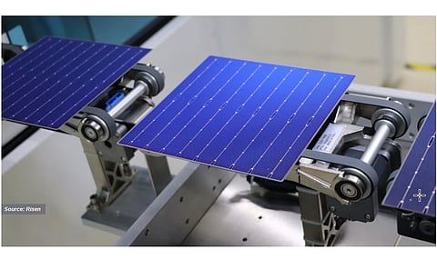
One of the most notable developments with respect to commercialization is that almost all mainstream PV manufacturers are involved in HJT to some degree, from R&D/pilot to commercial production. HJT has also attracted stakeholders that want to bring manufacturing to Europe. Strengthening of the supply chain is another important element. Not only are the production tools becoming ever more mature for mass production, the number of tool suppliers is also increasing. Equipment makers are also pitching in by introducing innovative tool platforms to improve throughput, supporting the processing of larger wafer formats, and thereby reducing costs. The special metallization pastes required are being optimized as well to reduce paste consumption and support higher printing speeds. In short, the supply chain is improving with more and more companies addressing the needs of HJT (see Progress Of Heterojunction Technology).
HJT is a low temperature-based process. The entire manufacturing process is accomplished at less than 250 °C, reducing the thermal budget of cell manufacturing. Moreover, the processing as such has fewer number of steps than PERC or TOPCon, with only 5 key processing stations.
This text is an excerpt from the TaiyangNews' Heterojunction Technology 2022 report, which provides an overview on the most recent HJT developments and can be accessed free of charge here.