

HJT is beginning to explore multi-cut designs, although its implementation differs from TOPCon because wafers are cut before cell processing
Tongwei demonstrated a module based on one-third cells, while Huasun indicated that multi-cut adoption remains part of its future plans
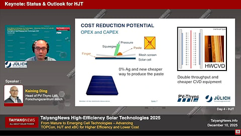
Future HJT roadmaps include thinner wafers, advanced passivation, pure copper paste and higher-capacity production lines
As Heterojunction (HJT) technology continues to evolve, manufacturers are looking beyond improvements in individual process steps. New cell layouts, thinner wafers and alternative materials are being explored to further improve performance and reduce manufacturing costs.
HJT is also following some of the design trends seen in TOPCon, such as multi-cut. However, the approach is not identical to TOPCon. Christian Comes, Head of Business Development Europe, Huasun indicated that the company is reserving the adoption of multi-cut formats for future development, as current incremental improvements are already delivering the required benefits. However, Tongwei has already tested the waters. The company developed a module based on a 3-cut configuration. The difference with HJT is that, unlike TOPCon, in which cells are fully processed and sliced before modules, HJT facilitates half-wafer processing, i.e., cutting the wafer instead of the cells. This also means that processing 3-cut wafers requires adaptations to production tools along the lines. Tongwei’s demonstration of making a module with a 1/3rd cell with a 790 W highlights the possibility of this adaptation (see HJT Manufacturers Look Beyond Metallization For Cost Savings).
The HJT segment also shows some consensus on future developments. Po-Chuan Yang, Dean of Global Photovoltaic Research Institute at Risen Energy outlined the key elements of the next phase, referred to as third-generation HJT, with these developments expected to take place beyond 2026. This includes the use of advanced microcrystalline passivation, next-generation tandem ITO targets, and the introduction of pure copper paste. On the wafer side, thickness is expected to go below 110 μm. At the same time, single shop-floor cell production capacity is projected to exceed 10 GW. With these developments, module costs are expected to become more competitive, potentially RMB 0.02/W lesser than those of mainstream technologies.
The text is an edited excerpt from TaiyangNews’ report on Cell & Module Technology Trends 2026, which can be downloaded for free here.
