

Sb-based photodetectors rely on single-crystal growth or solvent-based processing, limiting scalability and compatibility with industrial manufacturing
The study demonstrates room-temperature RF magnetron sputtering as a solvent-free method to deposit phase-pure Cs₃Sb₂Br₉ and Cs₃Sb₂I₉ thin films at the wafer scale
The resulting wafer-scale photodetectors achieve up to 3.3 A/W responsivity, along with strong uniformity and ambient stability
Lead-based perovskites have achieved high efficiencies in recent years, yet their long-term environmental footprint remains a subject of debate. In large-area devices and end-of-life disposal scenarios, concerns over metal toxicity and lead content present regulatory challenges that cannot be overlooked. Hence, attention is shifting toward lead-free compositions that maintain good optoelectronic performance while supporting commercially relevant production routes.
A recent study published in Advanced Science directly addresses this gap. According to the study, the highest device efficiencies have been achieved using single-crystal growth, a method that poses clear limitations for scalable, large-area production. In contrast, solution-based approaches reduce costs but depend on toxic solvents and struggle to deliver consistent film uniformity and phase control. Chemical vapor deposition, on the other hand, requires elevated growth temperatures due to differences in precursor volatility, thereby restricting substrate compatibility and increasing process complexity.
Among the proposed alternatives, antimony-based perovskite analogues such as Cs₃Sb₂Br₉ and Cs₃Sb₂I₉ have attracted interest. This is largely because, unlike tin-based compositions, which suffer from rapid oxidation of Sn²⁺ under ambient conditions, antimony (Sb) based materials exhibit improved chemical stability. Improved stability alone does not resolve the scalability challenge. Converting these materials from lab-scale demonstrations into manufacturing-ready thin films is still a key obstacle. To overcome this barrier, researchers use RF magnetron sputtering – a vacuum-based deposition method already common in semiconductor production. The solvent-free process enables direct growth from stoichiometric targets, improving process control and scalability for Cs₃Sb₂X₉ films.
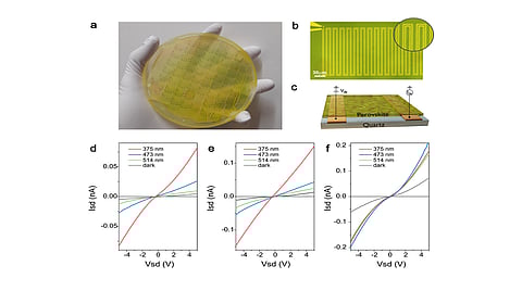
Using this approach, Cs₃Sb₂Br₉ (CSB) and Cs₃Sb₂I₉ (CSI) films approximately 300 nm thick were deposited directly onto 4-inch quartz wafers. Importantly, crystalline films formed at room temperature, demonstrating that high-quality Sb-based perovskite analogues can be synthesized without thermal assistance. To further understand the influence of temperature, a secondary growth condition at 150°C was introduced for comparison. Temperature-dependent growth also influenced microstructure. For the bromide-based films (CSB), the heated substrate resulted in a smaller average grain size (70 nm) compared to the room-temperature process (120 nm), a phenomenon attributed to a higher density of nucleation sites at elevated temperatures. Even under these differing conditions, no post-deposition annealing was required.
Structural analysis verified successful film formation. Raman spectroscopy further validated phase consistency. Optical measurements identified direct bandgaps of roughly 2.1 eV for Cs₃Sb₂I₉ and 2.6 eV for Cs₃Sb₂Br₉, situating both materials in the UV-visible range.
Having established structural and optical integrity, researchers then evaluated device performance, though metrics varied by composition. The sputtered films were integrated into planar photodetectors fabricated across full 4-inch wafers. Device uniformity was strong, with variation across the wafer remaining below 14%, indicating consistent film quality at scale.While the bromide-based devices operated efficiently in the milliampere-per-watt range, the iodide-based (CSI) devices reached values in the ampere-per-watt range under similar operating conditions.
Under low-intensity UV illumination, Sb-based photodetectors demonstrated photoresponsivity in the ampere-per-watt range, with peak values reaching 3.3 A/W. In addition to high responsivity, the devices demonstrated a specific detectivity in the 10¹⁵ Jones and a remarkably wide linear dynamic response of 165 dB.
The findings are detailed in the paper titled “Wafer-Scale Room-Temperature Processing of Lead-Free Perovskites for Optoelectronic Applications,” published in Advanced Science.
