

This is the second part on PECVD production equipment suppliers for HJT solar cell processing, which follows on article published last week that covered Chinese suppliers (see The Supply Side Of PECVD Tools For HJT – Part 1).
Among the non-Chinese companies, H2GEMINI is very interesting. Although very new in comparison to its peers, H2GEMINI's founders, the brothers Uwe and Dirk Habermann have more than 15 years' experience in building turnkey solutions for cell production across the world, and the design team has 40 years of experience in vacuum process technologies. H2GEMINI is mainly partnering with leading Chinese module equipment supplier Jinchen in China over its PECVD technology.
Emphasizing the fact that HJT involves depositing very thin layers which are very sensitive to contamination and mechanical stress due to handling, touching the wafer is a "no go," according to H2GEMINI CTO Dirk Habermann. The typical instances of wafer touching that need to be avoided are during loading/unloading, transporting from chamber to chamber and moving. Addressing this shortcoming, H2GEMINI has developed simple automation alongside the PECVD tool. With its so-called tray-less transport, wafers are placed on hangers, which are connected to the cell only at the edges and transferred into the chamber. A lift-up table then takes the wafers only by their weight. Subsequently, the hanger moves out, while the lift-up table moves down into the tray. The process goes in reverse post-deposition. This way, the tool handles the entire matrix of 10×10 of G12 wafers or 20×20 of half G12 wafers. This matrix handling completely avoids moving the wafers on the surface. Unlike with the majority of the tools, the wafer tray in H2GEMINI's PECVD reactor does not move during the deposition process. The other specialty of the tool is that the tray also does not move out of the deposition chamber, thus avoiding the need for preheating of the carrier. In addition, during the loading process, the wafers are heated to the process temperature by thermal radiation from the process chamber before they are actually placed in the tray, eliminating the lengthy preheating step in a separate chamber. All this collectively helps the tool to reach a cycle time of 60 seconds, which leads to an hourly throughput of 6,000 wafers for the G12 format. H2GEMINI is very secretive about its reactor design, but Habermann did provide a few details. The company's PECVD platform can support the deposition of both the amorphous as well as the microcrystalline silicon absorber layer. The PECVD developed in the joint venture by H2GEMINI and Jinchen is already in use at one of the early HJT adopters in China, according to the company without providing details.
Jusung Engineering from South Korea, with a long history of building vacuum deposition tools, has also developed key tools for HJT processing. However, only a few details are known from a product brochure of the company. The company's PECVD system can support the deposition of doped and intrinsic amorphous layers on 4,000 wafers per hour of M6.
While not offering a system specifically designed for heterojunction PV production, Applied Materials' PECVD tools designed for FTP can be tweaked for the deposition of doped and intrinsic amorphous silicon layers. The older generation of these tools were used by a few companies during the initial stages. However, these tools are not part of the plan for their next phase of expansions, but reportedly Enel has opted for AMAT's equipment for the first stage of its 3 GW expansion.
Debottlenecking: While PECVD was the main bottleneck for the throughput of a HJT line, the latest generation tools from a few suppliers address this with throughputs ranging from 6,000 to 7,200 wafers per hour even for G12 (full cell) format. (Source: TaiyangNews)
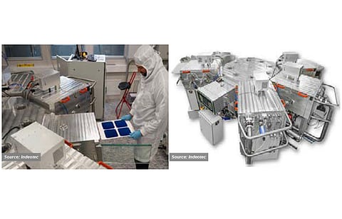
Switzerland-based INDEOtec is promoting an R&D tool platform, mainly for research centers and universities, at least as of now. The company's current offering is Octopus II, which is an R&D reactor that can be PECVD, PVD or a combination. The PVD is generally an inline machine with several chambers and PECVD is based on a cluster design. The company has also started offering a single module PECVD, which is exactly the same process module as that of the cluster tool, but it's basically a single load lock. The tools of the company can deposit both amorphous silicon as well as microcrystalline silicon. The company is offering two different variants of the PECVD reactor. The so-called classic design uses a carrier size of 35 x 45 cm – and can accommodate 4 M6 wafers and only 2 for any larger sizes beyond – to accomplish deposition on a single side. The reactor can reach temperatures of between 350 °C and 400 °C. INDEOtec has also developed a unique deposition method called Mirror PECVD that can completely avoid breaking the vacuum for flipping the wafers between the top and bottom deposition of amorphous silicon layers. To avoid the risk of dopant contamination in the intrinsic films from the previous deposition step, the company has developed a special method called Anti-Cross-Contamination-Treatment (ACCT). The combination of its ACCT and Mirror Reactor concepts allows the deposition of all four thin-film layers on the top and bottom of an HJT cell in the same reactor.
INDEOtec has installed 10 machines at leading research institutes, by which the company claims highest market share in equipment supply to the R&D segment of HJT. The company has been working on a mass production tool, called Octopus III for some time, for which the company is changing the tool configuration from cluster to inline; however, its release timeline remains unknown .
CAT-CVD, also known as hot-wire CVD, was also a widely used technology for core layer deposition. With this method, deposition species are generated by the catalytic cracking reaction of source gases on the heated catalyzer, instead of the collision between high energy electrons and molecules of source gases as with PECVD. Since the processing environment is free from ion bombardment, the resultant film is of high quality. The technology also carries the legacy of being used by Panasonic in the past. On the flip side, it is generally believed that increasing the throughput of the CAT-CVD tools is not easy and the tools themselves are not known for being handling-friendly, which means that automation costs are high. Moreover, due to the vertical processing design, breakages are also high. The hot wire "filament" requires special attention, involving higher maintenance costs. (see The Core Story Of HJT).
As of now, only Ulvac is offering a commercial-scale production system based on CAT-CVD, and we are not aware of any updates to the system after 2019, at which time the tool could process 180 M2 wafers per batch in 200 seconds. The total deposition area is 1,700 x 1,560 mm that enables processing 3,240 wafers per hour. There are also no updates regarding JAIST's proposed second generation CAT-CVD, the details of which were discussed in depth in our previous edition of the report.
PEALD is another alternative to PECVD, developed and promoted by China's Leadmicro. However, the company is now focusing more on the deposition of tunnelling oxide and polysilicon for TOPCon, another important application of the technology.
The Text is an excerpt from 3rd edition of TaiyangNews' Heterojunction Technology 2022 report, which provides an overview on the most recent production equipment developments. For more details, please read the full report, which can be accessed free of charge here.