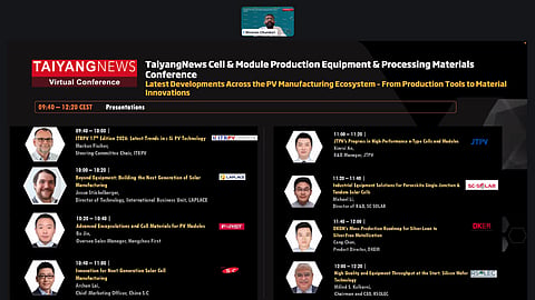


The ITRPV roadmap and the conference panel expect TOPCon to remain the dominant cell technology in the near to medium term, while BC and tandem technologies gradually gain market share
LAPLACE highlighted integrated factory solutions for TOPCon with AI-based process management along with full production lines for BC and tandem pilot lines
China S.C presented turnkey lines for TOPCon, HJT, and BC, with its latest developments focusing on high-throughput vertical LPCVD equipment and ultrathin HJT cells for space applications
JTPV outlined a roadmap combining multi-cut formats, edge passivation, and silver-lean metallization to raise TOPCon module power beyond 650 W, while advancing BC modules towards 700 W
Hangzhou First showcased specialized polymer films for 0BB and multi-cut functional inks for BC
DKEM presented a phased transition from reduced-silver pastes to silver-coated copper and ultimately pure-copper metallization, with commercial deployment already progressing in HJT and TOPCon production
SC Solar demonstrated production equipment designed to support the transition of single-junction perovskite and perovskite-silicon tandem technologies from pilot development to gigawatt-scale manufacturing
RSOLEC emphasized simulation, metrology, process optimization, and locally sourced consumables as important routes to improving crystal and wafer quality
PV technology has progressed remarkably. Initially aimed at enhancing quality and performance, technological progress later focused on cost reduction. Today, it is a crucial competitive edge and industry driver, especially amid manufacturing overcapacity challenges.
Meanwhile, regional technology roadmaps are diverging. Chinese manufacturers are advancing from first-generation TOPCon towards rear polyfingers and edge passivation. At the same time, back contact (BC) is not only gaining new followers, but is also being scaled to hybrid architectures. The industry’s long-term focus on perovskite-based tandem technologies persists, with increasing attention on pilot production and equipment preparedness. India’s growing manufacturing sector mainly concentrates on first-generation TOPCon, whereas Europe and North America explore a wider array of options including heterojunction (HJT) and tandem technologies.
At the module level, innovations are increasingly centered on multi-cut cell interconnection and gapless layouts. These advances owe much to the dedicated efforts of equipment manufacturers. Progress has also been seen in materials, particularly metallization pastes at the cell level and polymer wraps for modules.
Against this backdrop, the TaiyangNews Cell & Module Production Equipment & Processing Materials Conference 2026 convened equipment producers, material suppliers, and PV manufacturers to discuss manufacturing advancements. The event featured insights from three equipment companies, two material providers, and one manufacturer, and included representation from the upstream ingot and wafer sectors, along with a bird’s-eye view of technology progress from an industrial roadmap.
Opening the conference, Shravan Chunduri, Head of Technology at TaiyangNews, emphasized that the industry now has three major commercially available cell technologies – TOPCon, HJT, and BC – each supported by multi-gigawatt production capacity. At the same time, several companies are entering the pilot-production stage for next-generation tandem technologies. He stressed that these developments, along with continued progress at the module level, would not have been possible without the sustained efforts of equipment manufacturers and material suppliers.
ITRPV Expects TOPCon to Remain Dominant Through 2036
Providing a longer-term perspective, Markus Fischer, Steering Committee Chair of the International Technology Roadmap for Photovoltaics (ITRPV), presented key findings from the roadmap’s 17th edition. Based on contributions from 38 organizations and covering 70 parameters, the report assesses the industry’s status in 2025 and forecasts developments for the next decade, through 2036.
At the wafer level, n-type monocrystalline silicon already accounted for around 82% of the wafer market in 2025. Moving down the value chain to cells, TOPCon, which represented around 75% of cell production in 2025, is expected to remain the dominant technology over the forecast period. However, TOPCon-based back-contact technology is projected to expand its share from approximately 5% in 2025 to 23% by 2036. Silicon-based tandems could enter mass production around 2028 and account for 17% of the market by 2036. Over the same period, mass-produced module efficiency is forecast to rise from 23.9% to 25.2% for TOPCon and from 24.3% to 25.6% for TBC, while tandem modules could reach 31%.
Reducing material consumption will remain a central industry priority. Finer metallization patterns, process optimization and copper substitution are expected to lower silver consumption considerably. By 2036, silver use per M10 cell is forecast to decline to approximately 57 mg for TOPCon, 40 mg for HJT and 60 mg for TBC. HJT is expected to achieve the steepest reduction as copper-based metallization increasingly replaces silver.
Single-wafer traceability is also expected to become increasingly important for process control and defect identification. At the module level, lower degradation, longer warranties and operating lifetimes of up to 40 years are anticipated. The industry's learning rate also reflects the importance of continued innovation – between 1976 and 2025, module prices fell by an average of 26% each time cumulative shipments doubled. Looking to 2050, ITRPV’s broad-electrification scenario projects annual PV demand of more than 4.5 TW and cumulative installations of 63 TW (see ITRPV Sees PV Shipments Stabilize At 706 GW In 2025).
LAPLACE’s Focus on Integrated Factory Solutions
LAPLACE, a leading supplier of deposition and thermal-processing equipment, is expanding its offering through turnkey production solutions developed with partners. At the conference, Josua Stückelberger, Director of Technology for the company’s International Business Unit, focused his presentation on a general overview of equipment for TOPCon and BC cells, specific solutions for edge passivation and perovskite tandems, and integrated solutions for factories outside China.
He emphasized that establishing an overseas cell factory involves much more than supplying equipment and transferring processes. The company’s approach begins with defining the cell technology, capacity, output, yield, and quality targets. Manufacturers should then define the required equipment, automation, material flow, utilities, and infrastructure. “We don’t fit the factory into the building, but we design the building around the factory,” underscores Stückelberger. The approach offers many advantages, including reduced capital expenditure and space requirements, simplified utility connections, improved material flow, and faster production ramp-up. The presentation also emphasized an AI-based factory-management system that analyzes production data to detect process deviations, predict equipment issues, and recommend corrective action.
A key equipment highlight was LAPLACE’s Atomic Edge Passivation Deposition system for laser-cut cell strips. While cutting cells into smaller pieces reduces current and resistive losses at the module level, it creates unpassivated edges that increase recombination. The system applies a thin passivation layer to recover part of the resulting efficiency loss. For 210R-based modules, LAPLACE claims gains of at least 6 W for half-cut cells and 8.5 W for quarter-cut cells.
LAPLACE also offers thermal, deposition, laser, and automation equipment for BC pilot lines and mass production, with cumulative BC equipment shipments exceeding 100 GW. Looking further ahead, LAPLACE is developing a customizable 100 MW pilot line for perovskite and silicon–perovskite tandem cells. The company says its equipment has supported efficiencies of 24.01% for wide-bandgap perovskite cells and 33% for silicon-perovskite tandem devices.
Innovative Inks and Polymers from Hangzhou First
Following the conference agenda, Bo Jin, Oversea Sales Manager at Hangzhou First – an industry-leading supplier of PV encapsulation materials – discussed recent material innovations. He covered advanced polymer solutions for module manufacturing, including 0BB, edge sealants, buffer films for multi-cut cells, and insulation strips for string busbars. His presentation also featured solutions tailored for BC cell technology.
For 0BB modules, Jin explained that encapsulation materials must be selected based on how interconnection wires are attached to cells, which can be done in many ways. The company offers carrier film for both wire-foil interconnection, similar to smart wire connection technology (SWCT) from Meyer Burger and IFC, where the carrier film holds the wires onto the cell surface. The company also offers skin film for glue-based interconnection, where polymer strips keep the wire position intact until they are attached during lamination. For the 4th method, soldering + glue, Hangzhou First offers an integrated encapsulant with a one-sided low-flow property.
The company also presented a PIB edge-insulation solution for modules requiring ultra-narrow edge clearance. By using the edge seal as relied-upon insulation, the required creepage distance in a 1,500 V module can reportedly be reduced from 10.4 mm to 3.5 mm. For multi-cut modules, Hangzhou First introduced an EVA-based buffer film designed to cushion cut cells and reduce mechanical stress during lamination. It also presented a multilayer EVA-PET strip that electrically separates string busbars from underlying cells. It also improves adhesion and facilitates better resistance to microcracks.
At the cell level, Jin highlighted insulating and protective inks for BC technology. The insulation ink is applied to contacts of one polarity in an interdigitated pattern to realize a line soldering of the opposite polarity. Hangzhou First also developed a protective ink that prevents scratching of the cell surface when stacked for packing. The approach avoids the use of protective paper. Another material solution for BC is patterning ink. One variant of this ink is specially designed for BC to realize interdigitated p- and n-doped regions with an etch-and-resist approach, an alternative to laser ablation. Another variant can be used for copper plating, especially for HJT.
Vertical LPCVD for TOPCon and p-Type HJT for Space from China S.C
Archon Lai, Chief Marketing Officer of China S.C, presented the equipment supplier’s latest developments for TOPCon, HJT and BC cell production. The company provides turnkey lines for all 3 technologies, covering factory design, equipment installation, commissioning and production ramp-up.
Lai described TOPCon as the most mature and cost-effective option, with current mass-production efficiency estimated at 25.5% and the potential to reach 26.8%. BC offers the highest efficiency potential, rising from around 26% today to a projected 27.2%, although its estimated 92% production yield and higher silver consumption indicate that it remains less mature. HJT production efficiency is currently placed at 25.5%, with potential to reach 27%. Its estimated yield is 96%, while equipment investment is considerably higher than for TOPCon.
A key equipment highlight was S.C’s vertical cylindrical LPCVD system for TOPCon polysilicon deposition. As indicated, the tool uses vertically arranged process chambers, in contrast to conventional horizontal quartz-tube systems. The reactor supports wafer sizes up to 230 mm. According to the company, the design can process roughly three times as many wafers per chamber. In a 10 GW factory configuration, it could reduce equipment floor-space requirements by 33%. S.C also claims reductions of 32% in gas consumption, 15% in energy use per cell, and 78% in operation & maintenance effort. The quartz-tube-free design, more uniform temperature control, and semi-automated component replacement are intended to further simplify maintenance.
For HJT, the company is developing automated G12 production solutions. A recent technology upgrade is ultrathin cells for space PV and other weight-sensitive applications. Lai presented an n-type G12 half-cell with 25.5% efficiency and a power-to-weight ratio of 1.9 W/g on a pilot line, with thickness reduced from 60 µm to 50 µm. Separately, S.C is developing a p-type HJT cell using existing equipment and a front-junction structure. The 60 µm cell has achieved approximately 24.5% efficiency, with further process optimization underway.
Progress with TOPCon Generations and BC
Representing the manufacturer’s perspective on technology and production equipment, Xinrui An, R&D manager at leading PV manufacturer JTPV, presented the company’s progress in high-performance n-type TOPCon and BC technologies. JTPV operates two production bases with a combined annual capacity of 44 GW and reports cumulative cell shipments exceeding 116 GW.
For TOPCon, An outlined the evolution of JTPV’s cell technology platform – MoNo. The first generation combines optimized deposition, contacts, antireflection coatings, and fine-line metallization, achieving average cell efficiency above 25.5%. MoNo 2 adds a wave-shaped back-surface field, which is essentially poly-rear fingers and half-cut edge passivation, increasing efficiency by 0.4 to 0.5 percentage points. This resulted in a claimed module-level gain of 5 to 8 W. MoNo 3, currently in final pilot production, moves to multi-cut cells with fully passivated edges and silver-lean rear contacts. JTPV expects this design to deliver an additional 8 to 10 W and support its roadmap towards TOPCon modules exceeding 650 W.
An’s presentation also highlighted the company’s progress with BC. JTPV began developing TOPCon-based BC cells in 2023 and has since raised average cell efficiency from around 25% to 27.1%, with an in-house champion result of 27.4%. Its latest cells correspond to module power approaching 660 W in a 66-cell, 210R double-glass format.
JTPV also presented its busbarless Full Line Soldering design, in which ribbons are soldered directly to the underlying fingers. The company claims that this approach can reduce silver-paste consumption by more than 40% and bill-of-materials (BOM) costs by over CNY 0.05/W. On the performance side, this adds 5 W to module power and improves bifaciality by 10%. Further cell and module optimization has lifted bifaciality to approximately 75%. Although upgrading existing TOPCon capacity to BC requires additional patterning and wet-chemistry processes, An estimates that around 40% of its equipment can be reused. Its longer-term roadmap combines multi-cut cells, edge passivation, high-density layouts, and lower-temperature metallization, with module power potentially approaching 700 W.
SC Solar Targets GW-Scale Perovskite and Tandem Production
As perovskite technologies move from laboratory development towards industrialization, equipment suppliers are preparing solutions that bridge pilot production and gigawatt-scale manufacturing. Michael Li, R&D director at SC Solar, a well-known module production equipment supplier that ventured into supplying tools for perovskite production, presented the company’s turnkey equipment portfolio. The solutions include single-junction perovskite as well as perovskite-silicon tandem cells and modules.
For pilot production, SC Solar offers a 300 × 300 mm turnkey line integrating all key steps, from substrate cleaning and various treatment and deposition processes (including lasers and lamination) to characterization. For large-area perovskite production, SC Solar has developed line concepts for 600 × 1,200 mm and 1,200 × 2,400 mm substrates. The lines are designed to process approximately one panel per minute and combine slot-die coating and vacuum crystallization with PVD, ALD, evaporation, annealing, and laser processing. SC Solar’s PVD portfolio includes vertical and horizontal magnetron-sputtering systems for depositing layers such as nickel oxide, ITO, and copper. The modular platforms can be configured according to the required layer sequence, substrate dimensions, throughput, and factory layout.
For perovskite-silicon tandem production, the company presented an inline vacuum drying and crystallization system compatible with G12 wafers and upstream inkjet coating. With a throughput of 500 wafers per hour, the equipment uses recipe-controlled pressure and airflow profiles to manage film formation. The portfolio extends to a complete module assembly line, including conductive-tape and busbar application, glass pairing, butyl sealing, lamination, framing, junction-box processing, and final testing. The specialty of its flexible lamination platform is its interchangeable tooling, which accommodates different module formats, including single-junction perovskite and 2-terminal and 4-terminal tandem modules. Li said SC Solar has delivered and secured acceptance for 7 complete production lines, including equipment supplied to China, Europe and the US.
From Silver-Lean to Silver-Free Metallization from DKEM
Reducing silver consumption was the central theme of the presentation by Cong Chen, product director at DKEM. The company’s metallization roadmap begins with lowering paste consumption through fine-line, stencil, and transfer printing before progressing to low-silver formulations, silver-coated copper, high-copper pastes, and ultimately pure-copper metallization.
Copper offers good electrical conductivity at a considerably lower cost and with greater availability. However, the metal oxidizes more readily and can diffuse into silicon, causing recombination and performance losses. DKEM therefore develops copper metallization as a complete system covering paste formulation, printing, sintering, cell contacts, module sealing, and reliability testing.
HJT is currently the company’s most mature copper application. DKEM began gigawatt-scale production of silver-coated copper pastes for HJT in June 2023 and says the technology has reduced silver consumption from around 18 mg/W to 3-5 mg/W. The approach has also been adapted to HTBC cells, although their polished rear surface presents additional adhesion and contact-resistance challenges. For TOPCon, DKEM presented a double-printing process combining a thin silver seed layer for cell contact with a thicker silver-coated copper layer for current transport. The company claims that this configuration reduces effective silver consumption by approximately 50% without compromising cell efficiency. The process has entered mass production on three cell manufacturing shop floors, covering around 40 GW of cell capacity.
DKEM is also developing pure-copper pastes for HJT, HTBC, TOPCon, and TBC cells. While HJT and HTBC are more compatible with copper due to the presence of transparent conductive oxide, TOPCon and TBC still require a silver seed layer to act as a barrier. To address oxidation and copper-diffusion risks, DKEM uses a hybrid passivation system and proposes a moisture-resistant butyl module sealant. Its copper-paste module solution completed testing at three times the standard IEC duration in 2025, while undergoing field validation. Chen therefore positioned pure copper as an emerging industrial option, with silver-coated copper for HJT and copper-rich double printing for TOPCon already closer to broad commercial deployment.
RSOLEC Outlines Quality Roadmap for Crystal Growth and Wafering
Moving upstream in the PV value chain, Milind S. Kulkarni, Chairman and CEO of RSOLEC, outlined a quality and productivity roadmap for crystal growth and wafering. He emphasized that TOPCon, HJT, BC, and future perovskite-silicon tandem technologies impose different wafer requirements, particularly for oxygen concentration, resistivity, and defect control. These specifications must largely be achieved using existing Czochralski crystal-growth and diamond-wire-saw platforms, even as the industry transitions towards larger and thinner wafers with lower kerf losses. That’s because, unlike the downstream, there is no mainstream technology choice for this stage of the PV chain.
Kulkarni presented a roadmap for increasing output from existing equipment while reducing production costs by 30% to 40%. The proposed improvements combine equipment and mechanical modifications with process optimization, advanced control algorithms, simulation and the localization of key consumables.
At the crystal-growth stage, manufacturers must tightly control crystal diameter, dislocations, oxygen, resistivity, impurities, and microdefects. Continuous Czochralski growth could provide a more uniform resistivity profile than conventional batch processing, although oxygen incorporation remains a critical challenge. Kulkarni noted that simply lowering overall oxygen content may not prevent oxygen precipitate formation, which can reduce minority-carrier lifetime after high-temperature cell processing. RSOLEC’s simulations and experiments showed that process adjustments within the same crystal puller can significantly influence temperature distribution, melt flow, the crystal-melt interface and oxygen concentration.
Similarly, diamond-wire selection and slicing conditions affect wafer geometry, surface properties and subsurface damage, influencing subsequent texturing and cell processing. Kulkarni therefore stressed the importance of building in-house simulation and metrology capabilities. RSOLEC also plans to localize graphite, quartz and other crystal-growth consumables, which account for an estimated 15% to 20% of crystal-growth costs excluding polysilicon.
Panel Discusses Technology Adoption and Manufacturing Challenges
The conference concluded with a panel discussion examining the prospects, mainly for TOPCon and BC technologies, as well as the cost and investment considerations influencing their adoption. The panelists broadly agreed that TOPCon is likely to remain the leading cell technology in the near to medium term, supported by its mature supply chain, established manufacturing ecosystem and comparatively attractive production economics.
Sukumar Madugula, Sales Director at RCT Solutions, who joined the panel exclusively, noted that the industry has largely focused on TOPCon, with increasing innovation now occurring in materials, for example, copper metallization. JTPV’s An expects TOPCon to retain its dominant position for at least another five years, particularly in utility-scale applications. BC could gain a stronger foothold in the rooftop segment because of its higher front-side output and improved appearance, while HJT may remain focused on specialized applications such as space PV, where thin wafers, low weight, and high efficiency can justify its higher investment cost. Stückelberger said BC requires tighter control of temperature, gas flow, and film uniformity than TOPCon, making consistent mass production difficult.
Regional investment priorities also differ. Indian manufacturers remain strongly focused on capital expenditure, production volume, yield, and commissioning speed, making TOPCon the likely choice for most new projects over the next three to five years. In the US, bankability and rapid production ramp-up are additional considerations. A reliable TOPCon line that can be upgraded later may therefore offer a lower-risk entry point.
The panel identified copper metallization as an important route to reducing TOPCon costs and dependence on silver. Silver-coated copper is approaching commercial readiness, while pure-copper solutions still require further development to address process compatibility and reliability.
For BC, the main obstacles remain process complexity, yield, and translating laboratory results into stable mass production. With only about 40% of existing TOPCon equipment potentially reusable, the panelists suggested that BC may be better suited to new production lines or pilot projects than to complete factory conversions.
