
When wafers enter the core layer deposition stage, it means they reach the heart of HJT processing. This stop follows wet etching, which we discussed in a separate article (see Cleaning Has Big Role In HJT).
Core layer deposition involves multi-layer stacking of intrinsic-amorphous followed by doped-amorphous silicon layers of opposite polarities on each side of the wafer and controlling them at the nanometer scale. This is very important as the junction is created at the surface, and the deposited layers also dictate the effectiveness of passivation, which is key for HJT's high performance. Not only in terms of performance, as much as half of the CapEx required for the entire HJT cell processing line can be attributed to the core layer deposition tools. The importance and fundamentals of core layer deposition were discussed in depth in the previous editions of the TaiyangNews HJT report ( see Heterojunction Solar Technology 2022 Report); and as in the past, PECVD technology is still the state of the art for core layer deposition.
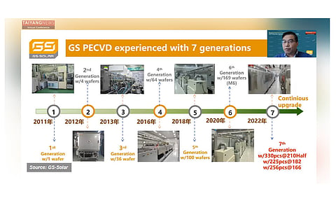
The most important development in the field of core layer deposition is the introduction of a microcrystalline silicon layer into the HJT structure. Implementing microcrystalline in the industry only refers to replacing the doped amorphous silicon layers, while the very thin intrinsic amorphous silicon films of 1 to 2 nm attached to the wafer surface remain the same. The primary advantage of using n-type microcrystalline silicon on the emitter side is that it can improve the current (Isc) and fill factor (FF). The increase in Isc is due to the fact that the light absorption coefficient of the microcrystalline silicon is far less than amorphous silicon. HJT devices that use microcrystalline silicon exhibit superior short and long wavelength responses. Risen says it will also introduce oxygen or carbon to increase the band gap within the microcrystalline layer for better short wavelength responses. The increase in FF is mainly due to the superior conductivity of the microcrystalline film, which decreases the silver resistance of cells and reduces the dependence on ITO for conductivity. The industry is also evaluating replacing p-type amorphous silicon with microcrystalline silicon on the rear side as the next step of improvement. Using a microcrystalline doped layer on both sides leads to high field effect passivation. The industry is colloquially referring to the amorphous silicon on both sides as HJT1.0, microcrystalline on the emitter side as HJT2.0, and double-sided microcrystalline as HJT3.0. At TaiyangNews' recent Solar Cell Production Equipment & Processing Materials conference (end-February), Jinyan Zhang, the GM at R&D department for GS-Solar, gave an insightful presentation on their specific PECVD solution for depositing microcrystalline silicon, titled Development of Micro-Crystalline HJT Solar Cells using 13.56MHz RF Mass Production Equipment (see recording here). Zhang emphasized that the 13.56MHz RF technology is ideal for large chamber PECVD equipment used in mass production of microcrystalline HJT cells, citing benefits such as good uniformity of the deposited films, a relatively wider and tolerant process window, and no plasma damage. He also presented raw production data that showed significant efficiency gains; a 0.5% efficiency gain with n-type microcrystalline silicon on emitter leading to an absolute efficiency of 24.47% and a further 0.4% gain by using the microcrystalline films on both sides that led to the efficiency of 25.45%. GS-Solar's latest 7th generation PECVD reactor has a capacity of 800 MW to 1 GW per single tool, and is capable of processing 330 half pieces of G12 wafers, a significant improvement over the previous generation tool's ability to process only 169 M6 wafers.
Maxwell, Ideal Energy Sunflower, and H2GEMINI are the other key tool suppliers in this segment. The PECVD tools from all these companies are able to support processing up to G12 size as well as half wafers, in addition to supporting higher throughputs of over 6,000 wafers of the same format (see Half Wafer Processing For HJT Cells). Among these, Maxwell's tool supports the highest level of 7,200 wafers per hour. Maxwells' vice president overseas sales Peter Wolf also presented the important features of the company's PECVD tools in his High Efficiency & Low Cost HJT Turnkey Line Solution talk at the TaiyangNews Conference (see presentation here). Top of the list is that the company uses 3 pieces of PECVD tools instead of the typically used 2. "We do i, i-n and p instead of typical i-n and i-p in 2 reactors," said Wolf, where I stands for intrinsic and n & p denote the 2 polarities of doping. This approach has 3 key benefits according to Wolf. The first is that the tray is not shared between i and p, which avoids boron-related contamination, thereby resulting in better passivation effect. Since the intrinsic layers are deposited first on both sides, the junction interface is protected while also avoiding phosphorus-related contamination on the p-side during the i-n coating. Finally, it also facilitates relatively higher i-layer deposition temperatures, improving the quality of the film.
For more details on HJT, download the TaiyangNews report on Heterojunction Solar Technology 2023 for free here.
