

One of the most significant wafer-related developments is half cell processing, which is becoming inevitable in the case of larger wafer formats for solar cells and modules, as shown in our monthly Top Module efficiency rankings. As discussed in the 3rd edition of our HJT reports, published in March 2023, the HJT segment, especially its entire production tool supply stream, though late, has successfully adapted to processing larger wafers.
Cutting of the cells is becoming a necessary step in order to counter resistance losses. On the other hand, the edge losses for HJT based on larger wafers, when processed into complete cells and then sliced, are higher compared to PERC due to the damages to TCO and also at the sliced edges. To address this problem, the equipment supply chain is now facilitating the processing of half wafers for HJT, meaning the wafer is sliced into half before cell processing, and these slices are then processed into cells. This approach brings in another benefit, which is the ability to process thinner wafers. As one could imagine, in the case of very thin and full wafers, the occurrence of wafer bending could be high. This can be avoided by cutting the wafer beforehand. At the line level, it is also easy for the automation to handle half-cut thin wafers compared to thin-full slices. These benefits are increasingly becoming hard to ignore, thus, it is now becoming part of the standard practice.
This is also the same with pre-annealing. In order to overcome the requirement for high wafer quality, the industry has adopted a heat treatment process (annealing) that mimics gettering, a process of removing metallic impurities with thermal treatment. As a result, HJT can now use wafers from different positions of the ingot and production runs of the crucible. Gettering also helps increase the yield of the whole line, according to Peter Wolf, VP overseas sales at the leading HJT tool vendor Maxwell. Thus, the heat treatment step is also becoming part of the process flow at leading production lines of HJT.
A very important wafer related topic for HJT is thickness reduction. This cell structure is highly compatible with thinner wafers, and its unique symmetrical structure only adds up to this benefit.
Po-Chuan Yang, general manager at Risen Energy's Business Unit HJT, shared the company's experience in its journey towards thinner wafers in its presentation Progress on HJT Technology and Key Milestones at Risen (see presentation here) during our TaiyangNews High Efficiency Solar Technologies 2022 event in Nov. 2022. Risen reduced the thickness in progressive steps of 10 μm, starting at 150 μm. However, each new step took longer than the previous one as several issues needed addressing, not only in cell production, but also in modules. For example, it took several weeks to hit 140 μm from 150 μm, a few months for the next 10 μm reduction and about half a year from then on to reach 120 μm. The company says that it now has a clear path towards 80 μm and is confident that it will enter mass production in the near future. In the meantime, Risen has already put 120 μm into production.
At the TaiyangNews HJT event, R&D director of solar cells at Huasun, Su Zhou shared his insights into wafer thickness reduction potential with respect to efficiency in his talk on Mass Production Status and Future Trends of HJT Solar Cells (see presentation here). The cell efficiency does not change notably while moving from 140 μm to 100 μm, according to Zhou. He further emphasized that the industrial goal for wafer thickness would be about 90 to 100 μm. Huasun has also started a wafer cutting facility and, according to Zhou, after several months of mass production experience, the equipment, material and process are now ready for 120 μm and 130 μm. On the 100 μm front, a cutting yield of 90% has been reached in the R&D line of Huasun's cutting lab, he said.
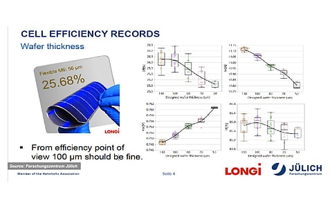
Kaining Ding, head of R&D department at the German research center Forschungszentrum Jülich (FZJ), in his conference keynote on the Status of HJT said that the mainstream wafer thickness was about 150 μm (during the end of 2022) and it is likely to go down to 125 μm; however, 100 μm is sufficient to achieve a cell efficiency of >26% (see presentation here). The main motivation behind reducing the wafer thickness is cost. To quantify the benefits, while it may not be absolutely accurate, a wafer price list from TCL Zhonghuan released in November 2022 offered some direction. It is public knowledge that n-type wafers are more expensive than p-type, and this price list indicates that the difference was about 6% at the time. This was determined by comparing the prices of n-type and p-type wafers of the same size (210 mm) and thickness (150 μm), given as 10.32 RMB and 9.73 RMB per piece, respectively. It is obvious that reducing wafer thickness reduces costs and enables companies to reduce prices as well. Again, this price list indicates that a 20 μm reduction in wafer thickness results in savings of 4.3% on wafer price, as indicated by the price of 210 mm wafers of 150 μm (10.32 RMB) and 130 μm (9.89 RMB). Thus, it is safe to say that if the n-type cell technologies can support a wafer that is 20 μm thinner, extra costs from the wafer side can be brushed off as negligible. The good news is that HJT, as it is, is able support this thickness delta with huge potential for slimming it down further.
For more details on HJT, download the TaiyangNews report on Heterojunction Solar Technology 2023 for free here.
