

In the third article on metallization of HJT solar cells we focus on plating as an alternative to incumbent screen printing. This follows on a recent article on HJT metallization discussing the status quo of HJT metallization including the fundamentals, approaches and key tool suppliers (see Silver Coated Copper Pastes For HJT); and a first one providing an overview on the main technology developments within the HJT metallization segment (see Looking Into HJT Metallization).
As with screen printing, plating also needs to be tweaked to be HJT-compatible. The need arises due to the presence of TCO on the surface of the solar cell, which is conductive. In the case of diffused junction cells, the passivation and anti-reflective dielectric film acts as a mask, enabling self-alignment. Thus, instead of the well-known light-induced plating, it is electroplating that is preferred here. The advantage of electroplating is that it makes bifacial plating possible. Intrinsically bifacial concepts such as heterojunction require the front and rear metallization to be done simultaneously, and electroplating addresses this need
Electroplating for HJT is based on a seed-and-plate approach, which can be realized in several ways. One is the deposition of a seed layer over the entire wafer surface and applying an organic plating mask. An alternative method is to apply a seed grid and using a dielectric as mask, where the conductive seed-grid is formed either through patterning of a sputtered seed layer or by printing of a metal paste.
The plating approach has its advantages. It is highly suitable for HJT given that it is a low-temperature process. It supports finer grid patterns of less than 25 μm, which reduces shading losses. The other aspect is a gain in conductivity. Although bulk copper is about 10% less conductive than silver, silver pastes are not pure themselves, and some organic residues always remain in the fingers. Thus, the conductivity of the fingers formed with copper plating is higher than the fingers formed with screen-printed silver paste. It can also be used in conjunction with standard soldering-based module interconnection technologies.
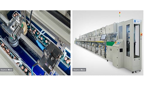
Meco, a division of Besi Group from the Netherlands, has been a longtime promoter of plating for HJT. Meco's plating system uses a proprietary inline concept based on vertical product handling with the help of a carrier belt. Optionally, the tool can also remove the mask and seed-metal layer. It can handle silicon substrates down to a thickness of 120 μm, and the average breakage rate is given as less than 0.1%. These basic attributes of the system have remained the same, the tool now has higher throughput and also compatible with larger wafers. While the system has a rated throughput of 6,000 wafers per hour for M6, it processes 4,500 G12 wafers per hour. Due to the higher throughput, the cost of ownership has decreased strongly to about 0.005 to 0.006 $/W, according to product manager Martijn Zwegers. Meco is working with material and other equipment suppliers involved in masking to make it more economical and simplified, an important cost consideration for HJT. The company is offering a "zero waste" version of the tool that doesn't need a plating license, according to Meco.
As mentioned earlier, HJT follows a seed-and-plate approach and all PVD suppliers are willing to extend their TCO deposition tools also to include the deposition seed layer (see TCO Deposition: First Foreign, Increasingly Local). VON ARDENNE and GS-Solar are extensively promoting this capability of adding this step into the PVD tools used for TCO deposition. Von ARDENNE in particular claims proven record with industry customers on the mass production of very smooth metal layer stacks since 2015. Two European R&D institutes – ISE & CSEM – have approaved the performance of the PVD solution of the company, according to Sebastian Gatz, Vice President Photovoltaics at VON ARDENNE. He further emphasizes the copper plating solution based on Von ARDENNE's has a 60% COO reduction potential compared to screen-printing technology.
Metallization is also a topic at TaiyangNews' upcoming annual flagship event, the virtual conference on High Efficiency Solar Technologies—TOPCon, HJT and Beyond, Today & Tomorrow to be held November 23-25, 2022. For free registration, please click here.
The text is an excerpt from 3rd edition of TaiyangNews' Heterojunction Technology 2022 report, which provides an overview on the most recent HJT developments as the technology is entering the GW scale production level and can be accessed free of charge here.
