- Nines PV from Ireland has developed a new technology to accomplish dry texturing without using plasma and vacuum
- The technology is applicable for every type of silicon solar substrate, but diamond wire sawn multicrystalline wafers would benefit the most
- The process, called ADE, is carried out at atmospheric pressure using fluorine as etch gas
- Nines PV’s technology is not only a single side process, but also offers control to realize different degrees of texturing
- The process enables realizing different scales of texturization reducing reflectivity from 19% down to 2%
- Nines PV is offering R&D and production scale products based on a modular design platform
Ireland-based equipment maker Nines Photovoltaics has developed an innovative dry texturing technology for solar wafers. The process is called ONYX, the company’s brand name for Atmospheric Dry Etching (ADE). The distinctiveness of the technology is that it accomplishes dry texturing at atmospheric pressure, eliminating the need for vacuum and plasma, which are the main ingredients of typical dry etching technologies. The technology is applicable for every type of silicon solar substrate; however, diamond wire sawn multicrystalline wafers would benefit the most from the technology. Nines PV is offering R&D as well as a production-scale product platforms.
Single side process
The ONYX texturing technology offers a new way of carrying out dry etching by employing gas at atmospheric pressure. The reaction zone of the reactor is isolated from the rest by means of gas curtains. The process is accomplished in an inline fashion. The wafers are fed to the machines by means of heated wafer carriers. An etching gas, which is fluorine (F2), is thermally activated in order to dissociate the molecules. The etchant is then delivered to the wafers through a specifically engineered distribution device in order to create the required etch depth, texture and uniformity. The setup enables single side processing. This decoupling provides the flexibility to opt for a different degree of texturing on the front and rear surface. More than that, single side processing is highly beneficial for advanced cell architectures such as Passivated Emitter and Rear Cell (PERC). The current practice in PERC processing is to apply the texturing on both sides, then the rear surface is again subjected to polishing. The ADE process is a drop-in replacement for the texturing process typically accomplished in wet-benches. In fact, wet-chemistry based solutions are also available for texturing diamond wire sawn multicrystalline wafers; Germany’s Schmid Group has recently introduced such a product (see Chemical Boost For Diamond Wire Sawing). However, Nine PV is mainly promoting its solution as an alternative to Reactive Ion Etching employed for dry etching.
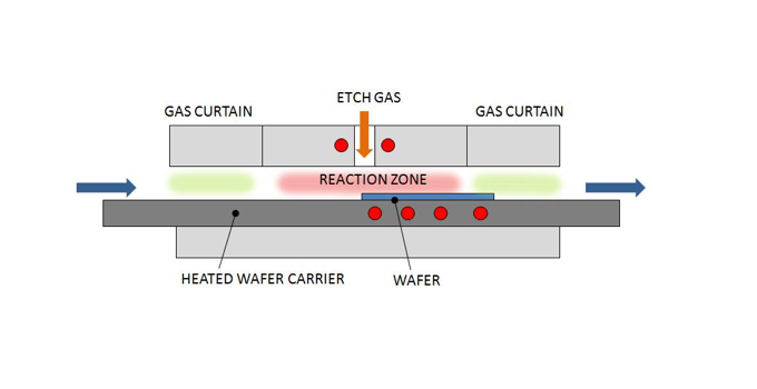
The dry etching technology developed by Nines PV uses fluorine as etching gas, which works on a single side, as shown in this schematic. (photo credit: Nines Photovoltaics)
Different degree of texturing
The atmospheric nature of the ADE process enables reaching high etching rates. For example, a wafer can be etched in less than a minute when using 30% concentrated fluorine and etching time can be decreased dramatically to few seconds using 100% fluorine. Nines PV’s technology accomplishes different types of texturization as well. The ADE can realize all the way from micro-scale texturing obtained with typical wet-benches down to black silicon level of nano-scale texturing leading to black silicon. The latter is typically accomplished with either Reactive Ion Etching (RIE) or Metal-catalyzed chemical etching (MCCE) type wet-chemistry. The technology enables attaining a wide range of reflectivity from 19% down to 2%.
The process is also compatible with different types of silicon substrates – mono, multi, quasi-mono, diamond wire-cut, slurry cut and thin epitaxial films or wafers. However, the diamond wire sawn multicrystalline wafers would have higher benefits. Diamond wire technology comes with great benefits of reducing manufacturing costs about 6 to 8 euro cents per wafer. However, when employed for sawing multicrystalline ingots, the resultant wafers have a smooth surface that is not susceptible for stand texturization. Thus ADE could be an enabling technology for widespread use of diamond wire sawing for multicrystalline wafers.
Being Green
According to Nines PV, its approach is a very environment friendly process. CTO Laurent Clochard emphasizes that the Global Warming Potential (GWP) of fluorine is zero, while SF6, the commonly used gas for dry etching, has a GWP of 22,800, which refers to a global warming potential related to CO2 and a lifetime of 3,200 years. Another common etching gas NF3 also has a high GWP of 17,200. On top, “We are using a dry process, without need for water, says Clochard.
Modular product platform
As for executing this process, Nines PV has developed a so called “open end” product platform, which allows continuous passing through of wafers during the process without any involvement of load locks and vacuum chambers. According to Clochard, after some R&D and proof of concept, the first full-scale prototype was built in 2013. The company then cooperated with Fraunhofer ISE on cell process integration. Last year, the company has been focussing on setting up new dry texturing pilot line facilities in Dublin, including a fully automated ADE tool, which is ready now, says Clochard. This would help the company to demonstrate the technology, especially on larger sample quantity.
When it comes to products, Nines PV is offering a R&D/pilot system, called 9sADE100, for developing the process. It uses low concentration of etching gas, which is supplied from high pressure bottles. The system is designed in such a way that when required it can be upgraded for industrial installation. According to Clochard, one of the key points of the Nines PV’s technology is scalability. A fully automated single lane version of the production scale tool has a throughput of 1,000 wafers/h. A multilane design, called 9sADE6000, can handle up to 6 parallel lanes with a throughput of 6,000 wafers per hour, which represents the top configuration.
The Gains
The major difference with the industrial tool is that it is equipped with on-site generation of etching gas to use 100% concentration. This on-site gas generation is offered by established gas companies, such as Linde and Solvay. “We usually bring them on board early in discussion with potential customers,” says Clochard. Nine’s PV technology also improves the cell performance, according to Clochard. This was demonstrated that ONYX texturing implemented on standard aluminium BSF cell technology has resulted in a 0.3% gain in efficiency over the acidic texturing process, with the results certified by Fraunhofer CalLab, the company says. As for the capex, Clochard says, the top configuration ADE tool with a 200 MW capacity ADE tool is priced at a “fraction” of typical RIE tools. The company did not provide the actual price.
On top, the technology would als support simpler operation and maintenance as there are no high-end power generators and vacuum pumps, and a simple wet scrubber can be used for effluent treatment, the company says. Taking all these factors into consideration, Clochard says, Nines PV’s ADE technology has the potential to reduce the total cost of ownership by 50% compared to available dry etching technologies.

