
- Markets
- Business
- People
- Opinion
- Technology
- Storage+
- Reports
- Our Events
- Tenders
- Price Index
- Top Modules
- ServicesServices
- AnalysisAnalysis

All advanced solar cell technologies have a different cell structure and follow a fairly different process flow. However, from a broader perspective, the passivation scheme is the key differentiating element for all these high-efficiency cell technologies. Tweaking the metallization process according to the passivation configuration is another important part of implementing all these advanced cell technologies. Below is a brief summary of the basics of passivation.
Basics of Passivation
The silicon wafer — the basic raw material — still has inherent defects at the time of entering a cell line. Most prominent are surface defects originating from the fundamental process of slicing the wafers from an ingot causing disruptions of a crystal lattice at both wafer surfaces. These interruptions in the periodical arrangement of silicon atoms result in so-called dangling bonds, working as recombination centers. Passivation is a process in which these defects are made inactive to reduce the surface recombination of charge carriers, safeguarding cell efficiency.
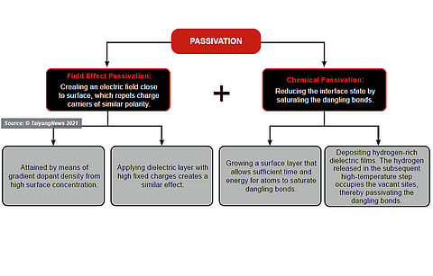
There are two complementing methods of passivation: a) strongly reducing charge carriers of one polarity reaching the surface, and b) reducing the interface state by saturating the dangling bonds. The latter can be accomplished, again, in two ways. One is to simply saturate the dangling bonds on the surface by providing suitable conditions to grow a surface layer that allows sufficient time and energy for atoms to reach optimal energy levels to saturate these dangling bonds. Alternatively, one can deposit a hydrogen-rich dielectric film that releases hydrogen in subsequent firing steps. The free hydrogen occupies vacant sites of dangling bonds, thereby pacifying them. This method is called chemical passivation.
There exists another mechanism called field effect passivation, which involves creating an electric field close to the surface that can repel the charge carriers of similar polarity. It can be achieved by means of descending dopant density from high surface concentration. On top, applying a dielectric layer with high fixed charges also creates an electric field gradient near the surface, which provides field effect passivation (see graph). Following this basic principle, every advanced cell architecture features a specific passivation scheme.
For in-depth details on TOPCon cell technology and advancements please download and read TaiyangNews free report on TOPCon Cell Technology here.
