

A very important wafer related topic for HJT is thickness reduction. The HJT cell structure is highly compatible with thinner wafers in various aspects. The wafer thinning in the first instance reduces the efficiency due to the losses in current, which can be compensated by reaching higher Voc with a superior passivation scheme on both sides. The uniqueness of HJT is also that it is a symmetrical structure, providing a superior amorphous silicon based passivation on both sides.
Another advantage of such a structure is that it prevents warpage during the process, avoiding physical breakages of wafers. PERC and even TOPCon in today's context are non-symmetrical structures, providing superior passivation on only one side, thus are less compatible with thinner wafers. HJT processing is mostly inline, another aspect that favors thinner wafers, while PERC and its TOPCon extension are mainly batch processes (see Wafers Side Of HJT).
On the flip side, HJT cannot directly support thin wafer processing. It also causes current losses; and replacing doped amorphous silicon layers with microcrystalline can pave the path towards thinner wafers, according to Huasun's CTO Wenjing Wang. Risen, sharing its experience adapting to thinner wafers, stated that it has started working with 120 μm as of Q2/2021, and the efficiencies at the beginning were lower than the baseline process due to the sudden decrease in current. But the introduction of microcrystalline doped layers not only helped recover the efficiency, further optimization resulted in even better efficiencies. Risen reduced the wafer size progressively in steps of 10 μm starting at 150 μm. However, each step took longer time than the previous one. For example, it took several weeks when going down from 150 μm to 140 μm, a few months for the next 10 μm reduction and about half a year from then on to reach 120 μm. The company said it now has a clear path towards 80 μm (see The Status Quo Of HJT Processing).
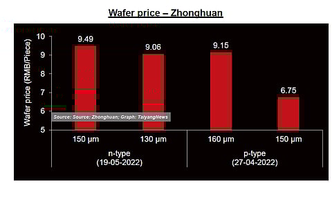
The main motivation behind reducing the wafer thickness is cost reduction, which has become even more significant with skyrocketing prices of polysilicon. The rationale is simple: thinner wafers reduce silicon consumption. In the past, at least until 2020, the rule of thumb was that a reduction of 10 μm in wafer thickness reduced wafer costs by $0.01. HJT typically uses a thickness that is 10 to 15 μm lower compared to mainstream p-type PERC. While the typical wafer thickness with PERC is about 160 μm, the first 150 μm cells have hit the marketplace as was observed at the recent Intersolar Europe, where Tongwei presented its cells. The majority of the HJT process lines are currently processing 150 μm wafers with plans in place to size it down further. Since wafer thickness reduction often goes hand in hand with new expansion plans and different companies are at different milestones, their roadmaps vary quite a bit. However, a recent price list (released on May 19, 2022) by TCL Zhonghuan, the second largest wafer supplier after LONGi, indicated some direction. Only two variants of n-type are listed, with the thickness being the only difference – 150 μm and 130 μm – and both are of G12 size. While the former represents the mainstream, the latter is perhaps the next step in thickness reduction. Zhonghuan's price list also indicates the price difference between the p-type and savings with thinner wafers. The G12 wafer with 150 μm had a price tag of 9.49 RMB/piece, while the thinner 130 μm variant was priced at 9.06 RMB/piece. Simplified, a 20 μm reduction in wafer thickness results in savings of 4.5% on wafer price. As to the gap between p-type and n-type wafers – a very important aspect of benchmarking HJT to PERC – are about 6% more expensive than p-type wafers of the same thickness (150 μm) priced at 8.95 RMB/ piece. This implies using thinner wafers, HJT can more or less compensates for the premice premium for n-type wafers.
The Text is an excerpt from 3rd edition of TaiyangNews' Heterojunction Technology 2022 report, which provides an overview on the most recent HJT developments as the technology is entering the GW scale production level and can be accessed free of charge here.
