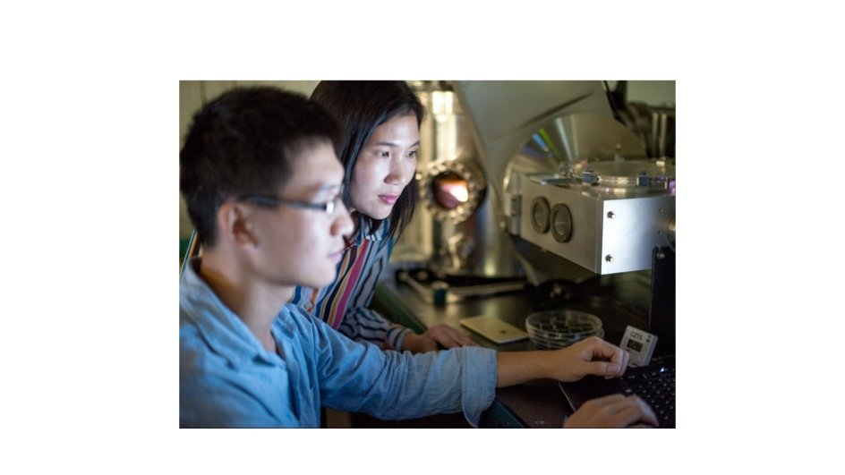
- UNSW’s Solar Energy Researcher Dr Xiaojing Hao and her team have broken the 10% efficiency barrier for sulphide kesterite or CZTS, which they tag the ‘solar cell material of the future’
- With plenty of copper, zinc, tin and sulfur, CZTS is a low-cost, flexible and non-toxic thin-film cell structure
- It might be used in the future as an alternative to CIGS structures using considerable amounts of expensive indium
- CIGS production processes can also easily adapt to producing CZTS, according to the research team
- Further research is required to improve efficiency of CZTS to be able to use it for commercial purposes
A research team at University of New South Wales (UNSW) in Australia has broken the 10% efficiency barrier for what it calls the ‘solar cell material of the future,’ sulphide kesterite. This is a compound comprising copper, zinc, tin and sulfur and is also referred to as Cu2ZnSnS4 or CZTS. According to UNSW, the record for this type of cell was stagnant for 9 years.
These findings, achieved by the team led by UNSW Solar Energy Researcher and Scientia Fellow Dr Xiaojing Hao, have been published in the journal Nature Energy.
CZTS is a thin-film semiconductor material derived from commercial thin-film structure CIGS. The indium used in this technology is relatively rare and in high demand for use in flat panel displays, hence expensive. But CZTS, with its zinc and tin properties available easily, can easily replace indium and gallium.
This gives a ‘low-cost, flexible, non-toxic and abundant’ option, said Hao. Adding, “In addition to that, as a stand-alone thin-film PV, CZTS related material has a chance to be used in a tandem cell with silicon as its bandgap can be easily tuned over a wide range when alloying with other elements, making it well matched to the high bandgap requirements for the upper cells of tandem stacks.”
In the Nature Energy publication, the team reports about a certified 11% efficiency Cu2ZnSnS4 solar cell with a high 730 mV open-circuit voltage using heat treatment to reduce heterojunction recombination. This heat treatment, they say, facilitates elemental inter-diffusion, directly inducing Cd atoms to occupy Zn or Cu lattice sites, and promotes Na accumulation accompanied by local Cu deficiency within the heterojunction region. Consequently, they further explain, new phases are formed near the hetero-interface and more favourable conduction band alignment is obtained, contributing to reduced non-radiative recombination.
Using this approach, the team said that it also was able to demonstrate a certified centimetre-scale (1.11 cm2) 10% efficiency Cu2ZnSnS4 photovoltaic device; the first kesterite cell (including selenium-containing) of standard centimeter-size to exceed 10%.
CIGS production processes are also CZTS ready, according to the scientists. What is now required for the material to be used commercially are improved efficiency levels, of beyond 20%. However, CIGS technology, which has reached record efficiencies of over 22%, is not competitive today with crystalline silicon wafer based cells today; its market share is negligible in the low 1-digit percentage range.
Given the advances in efficiency made in the past few years – from 7.6 per cent to 11% – Hao believes she and her team are on the right track to achieving efficiency levels of 15 or 20 %. She did not give a time frame.
She will be applying for funding for a new project at the end of the year to help further investigate the efficiency level improvement of CZTS.
Hao is also working on similar other ‘green materials’ that are easily available, non-toxic and could be used in tandem with silicon, along with Professor Martin Green who is known as the inventor of the silicon based PERC technology. Recently, Green won the Global Energy Prize for his pioneering work in the field of PV (see Martin Green Wins Global Energy Prize).


