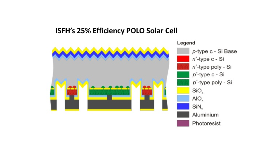
- ISFH attained 25% efficiency for lab-scale cell float-zone monocrystalline cell combining the POLO junctions concept with backcontact architecture
- The crucial aspects of the POLO contacts technology is: growth interfacial oxide, deposition of polycrystalline silicon layer, which is doped subsequently
- Interdigitated emitter and base regions are separated by textured trenches, which is key for adapting POLO contacts to backcontact cell concept
- Increasing efficiency further and industry relevant process steps are in focus for future development
The Institute for Solar Energy Research Hameln (ISFH) in cooperation with the Institute for Materials and Devices of Electronics (MBE) of Leibniz Universität Hannover have attained a remarkable solar cell efficiency of 25% for a float-zone monocrystalline cell. This high efficiency has been reached by adapting a ‘polycrystalline on oxide’ (POLO) passivating contacts concept onto backcontact cell architecture. The 25% efficiency corresponds to an open circuit voltage of 723 mV and a current density of 41.9 mA/cm2 realized on a designated area of 3.97 cm2 and using a p-type float zone silicon substrate. The results were certified by calibration lab ISFH-CalTec, which is accredited by DakkS and were presented at the Asian PVSEC-26 conference, held in Singapore end of October.
Passivating contacts is not new altogether. The well known heterojunction technology, which is the basis for world record efficient cells, such as from Kaneka at 26.3% and Panasonic’s 25.6%, is a very good example for the passivating contact approach. However, according to Felix Haase, ISFH’s head of the project that led to 25% efficiency, amorphous silicon/crystalline silicon heterojunction architectures suffers from an inherent limitation of low temperature processing. Thus standard procedures, for example metallization and interconnection, which are typically operated at higher temperatures need to be accomplished at reduced temperatures. The other disadvantages is parasitic optical absorption in the doped amorphous silicon layer and the need for ultra-clean wafer surfaces before the deposition of thin-film silicon layers. Combining heterojunction with backcontact structures also requires complex patterning procedures for the formation of interdigitated junctions.
Passivation unaffected
In an effort to address these limitations, ISFH has developed POLO passivating contacts that are stable under high temperatures. The crucial aspects of the POLO contacts are growth of interfacial oxide and deposition of intrinsic polycrystalline silicon layers, which are subsequently doped accordingly. The beauty of the approach, according to Haase, is that the junctions are resulting in low passivation current densities (1 fA/cm2 on n+-POLO and 4 fA/cm2 on p+-POLO), which can be contacted by metal without inducing any additional recombination losses. The contacted POLO junctions are often referred as POLO contacts.
Moving the technology into the backcontact domain required separation of base and emitter regions. ISFH employed textured trenches to separate evaporated aluminum contacts. The interfacial oxide can be grown thermally as well as by means of wet chemistry. Low-pressure chemical vapor deposition (LPCVD) systems available commercially are employed to deposit intrinsic polycrystalline silicon layer. The intrinsic layers are subsequently doped using ion implantation process, while in-situ doping in LPCVD is also possible, says Haase. Though the approach enables using industrially viable practices in principle, the current record cell has been processed using complex and high-end steps such as photolithography and metal evaporation steps.
Process Intricacies
- The process sequence has the following steps implemented on p-type float zone silicon substrate with base resistivity of 80 ohm.cm (see schematic) .
- Thermally growing interfacial silicon oxide on both sides
- Intrinsic polycrystalline silicon layers grown in LPCVD
- Boron implantation on rear side
- Photoresist masked phosphorus-implantation on front side and rear side, overcompensating the boron doping on rear
- Thermally grown silicon oxide as etch barrier for texture
- High temperature break-up of the interfacial silicon oxide layer
- Photoresist masked etching of silicon oxide as etch barrier for texture
- Texture of front side and trench areas separating p+/n+ poly-Si junctions
- Passivation of front and rear side with 20 nm ALD-AlOx Double antireflection layer PECVD-SiNy/PECVD-SiOz and PECVD-SiOz rear reflector
- Photoresist masked etching of rear dielectric for local contacts
- Removal of photoresist
- Thermal evaporation of aluminium + sputtered silicon oxide etch barrier
- Contact separation by wet chemical etching
Haase in his presentation at the Asian PVSEC noted that the best cell of the first batch realized with the above process flow had a conversion efficiency of 24.6%. Further investigation revealed that contact opening process degrades aluminum oxide passivation, especially due to thin layer of photoresist. The thin photoresist layer was not thick enough to protect the AlOx passivation in the trench area during wet chemical contact opening etch, says Haase. Then increasing the thickness of the photoresist layer has led to the 25% efficiency, while the simulations revealed that the technology has a potential to attain efficiencies up to 27%. The future plan is not just to increase efficiency, ISFH is also trying to replace the complex laboratory processes with industry relevant steps, paving a path to commercialization.
With standard procedures too
In fact, another research group from ISFH, led by Robby Peibst, developed a photolithography-free process sequence for POLO technology adapted to backcontact structure. According to a presentation at the 2nd HERCULES Workshop held in Berlin in October, this approach also relies on textured trenches to separate the emitter and base regions but employed inkjet and laser technology for patterning and contact opening, a mask free high throughput metallization process and a self aligned contact separation method. The process resulted in 24.25% best cell efficiency on n-type wafers. However, Haase says that the higher efficiency realized by his group is as a result of an advanced passivation scheme, especially employing aluminum oxide. Incorporating such a passivation configuration into a photolithography-free process would also enable a conversion efficiency of 25%.


